

 Home
Home
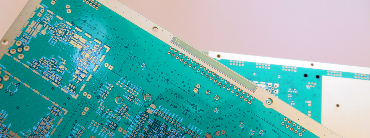
Rogers RO4350B 8-Layer 1.6mm HDI RF PCB with ENEPIG for RF Communications
This 8-layer rigid PCB utilizes Rogers RO4350B core material and RO4450F bondply, designed for high-frequency applications requiring precise impedance control
.jpg)
8-Layer HDI PCB Built On Tg175°C FR-4 Immersion Gold PCB for Satellite Radio Applications
This 8-layer HDI printed circuit board is engineered for high-frequency applications such as satellite radio systems, constructed on high-performance FR-4 Tg175℃ substrate
.jpg)
6-Layer HDI Circuit Board Via in Pad PCB 0.6mm Multilayer PCB via filled and capped for GPS Tracking
This 6-layer HDI PCB is a 0.6mm thick, FR-4 based board designed for GPS tracking devices.
.jpg)
10-Layer High-Tg FR-4 HDI PCB with Immersion Gold Finish for High-Density PLC Modules
This 10-layer HDI PCB is a high-performance board designed for PLC control modules.
Isola 370HR 6-Layer 1.6mm HDI PCB for High Density Industrial Electronics
This product is a high-reliability 6-layer HDI (High-Density Interconnect) printed circuit board engineered for demanding industrial and electronic applications.
IT-180A and FR-4 4-Layer 1.6mm PCB for Automotive Engine Room ECU and Telecommunications
This 4-layer rigid PCB is made of FR-4 (IT-180) base material, complying with IPC-Class-2 quality standards. This IT-180 and FR-4 PCB has a finished thickness of 1.6mm