
 Home
-
HDI PCB
-
8-Layer HDI PCB Built On Tg175°C FR-4 Immersion Gold PCB for Satellite Radio Applications
Home
-
HDI PCB
-
8-Layer HDI PCB Built On Tg175°C FR-4 Immersion Gold PCB for Satellite Radio Applications
8-Layer HDI PCB Built On Tg175°C FR-4 Immersion Gold PCB for Satellite Radio Applications
Printed Circuit Boards are custom-made products; the images and specifications provided are for reference only.
1.1 General description
This 6-layer HDI PCB is a 0.6mm thick, FR-4 based board designed for GPS tracking devices. It features advanced microvia technology, including blind vias (L1-L2) and buried vias (L3-L4), with all 0.25mm vias resin-filled and capped for via-in-pad design. The finish is Immersion Gold on pads with a green Taiyo solder mask, compliant with IPC-6012 Class 2. Panels are supplied 1-up by ITEQ and shipped in packs of 50.
.jpg)
1.2 Features and benefits
1. Via in pad design reduced the inductive reactance and capacitive reactance of the transmission line;
2. Immersion gold finish has high solderability, no stressing of circuit boards and less contamination of PCB surface;
3. Products and manufacturing are certified by authorized organizations;
4. Eligible products rate of first production: >95%;
5. Prototype PCB capability to volume production capability;
6. Delivery on time: >98%;
7. More than 18+ years of PCB experience;
8. IPC Class 2 / IPC Class 3;
1.3 Applications
Led Lighting
Intercom System
Portable WiFi Router
GSM Tracker
Commercial Led Lighting
Modem WiFi 4G
Honeywell Access Control
Electronic Access Control
Audio Frequency Amplifier
File servers
1.4 PCB Specifications
| PCB SIZE | 100 x 103mm=1PCS | |||
| BOARD TYPE | Multilayer PCB | |||
| Number of Layers | 6 layers | |||
| Surface Mount Components | YES | |||
| Through Hole Components | NO | |||
| LAYER STACKUP | copper ------- 18um(0.5oz)+plate TOP CS | |||
| 4mil prepreg | ||||
| copper ------- 18um(0.5oz) GND Plane | ||||
| 4mil FR-4 | ||||
| copper ------- 18um(0.5oz) PWR Plane | ||||
| 4mil prepreg | ||||
| copper ------- 18um(0.5oz) PWR Plane | ||||
| 4mil FR-4 | ||||
| copper ------- 18um(0.5oz) SIG | ||||
| 4mil prepreg | ||||
| copper ------- 18um(0.5oz) BOT PS | ||||
| TECHNOLOGY | ||||
| Minimum Trace and Space: | 3mil/3mil | |||
| Minimum / Maximum Holes: | 0.22/3.50mm | |||
| Number of Different Holes: | 25 | |||
| Number of Drill Holes: | 2315 | |||
| Number of Milled Slots: | 0 | |||
| Number of Internal Cutouts: | 0 | |||
| Impedance Control | no | |||
| BOARD MATERIAL | ||||
| Glass Epoxy: | FR-4, ITEQ IT140 TG>135, er<5.4 | |||
| Final foil external: | 1oz | |||
| Final foil internal: | 0.5oz | |||
| Final height of PCB: | 0.6mm ±0.1 | |||
| PLATING AND COATING | ||||
| Surface Finish | Immersion gold 0.025µm over 3µm Nickel (14.4% area) | |||
| Solder Mask Apply To: | TOP and Bottom, 12micron Minimum | |||
| Solder Mask Color: | Green, TAIYO PSR-2000 GT600D | |||
| Solder Mask Type: | LPSM | |||
| CONTOUR/CUTTING | Routing | |||
| MARKING | ||||
| Side of Component Legend | No silkscreen requried. | |||
| Colour of Component Legend | No silkscreen requried. | |||
| Manufacturer Name or Logo: | No silkscreen requried. | |||
| VIA | Plated through hole(PTH), Blind via and via capping on CS and PS, vias not be visible. | |||
| FLAMIBILITY RATING | UL 94-V0 Approval MIN. | |||
| DIMENSION TOLERANCE | ||||
| Outline dimension: | 0.0059"" (0.15mm) | |||
| Board plating: | 0.0030"" (0.076mm) | |||
| Drill tolerance: | 0.002"" (0.05mm) | |||
| TEST | 100% Electrical Test prior shipment | |||
| TYPE OF ARTWORK TO BE SUPPLIED | email file, Gerber RS-274-X, PCBDOC etc | |||
| SERVICE AREA | Worldwide, Globally. |
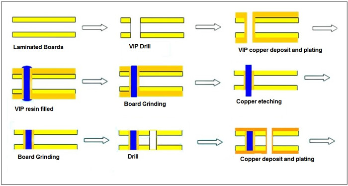
1.5 via in pad (VIP)
At present, the circuit board is becoming more and more dense and interconnected, and there is no more room for these wires and pads connecting the holes. Therefore, so in this context, the process of punching the holes on the pads arises at the historic moment. In brief, the via holes which have been plated through are plugged or filled by insulating resin through the method of screen leakage, and then drying, grinding, and then electroplating, so that the whole surface of the PCB is coated with copper, and no longer via holes can be seen.
The effect of via in pad is also very obvious: such as improved the electrical performance and reliability of electronic products, shorten the signal transmission wire, reduced the inductive reactance and capacitive reactance of the transmission line, and reduced internal and external electromagnetic interference.
Let’s see the basic process of via in pad.