

 Home
-
F4B PCB
-
F4BTMS1000 4-Layer 12.9mm HDI PCB with Blind Via Buried Vias for Microwave and Radar Applications
Home
-
F4B PCB
-
F4BTMS1000 4-Layer 12.9mm HDI PCB with Blind Via Buried Vias for Microwave and Radar Applications
F4BTMS1000 4-Layer 12.9mm HDI PCB with Blind Via Buried Vias for Microwave and Radar Applications
Printed Circuit Boards are custom-made products; the images and specifications provided are for reference only.
Overview of This Type of PCB
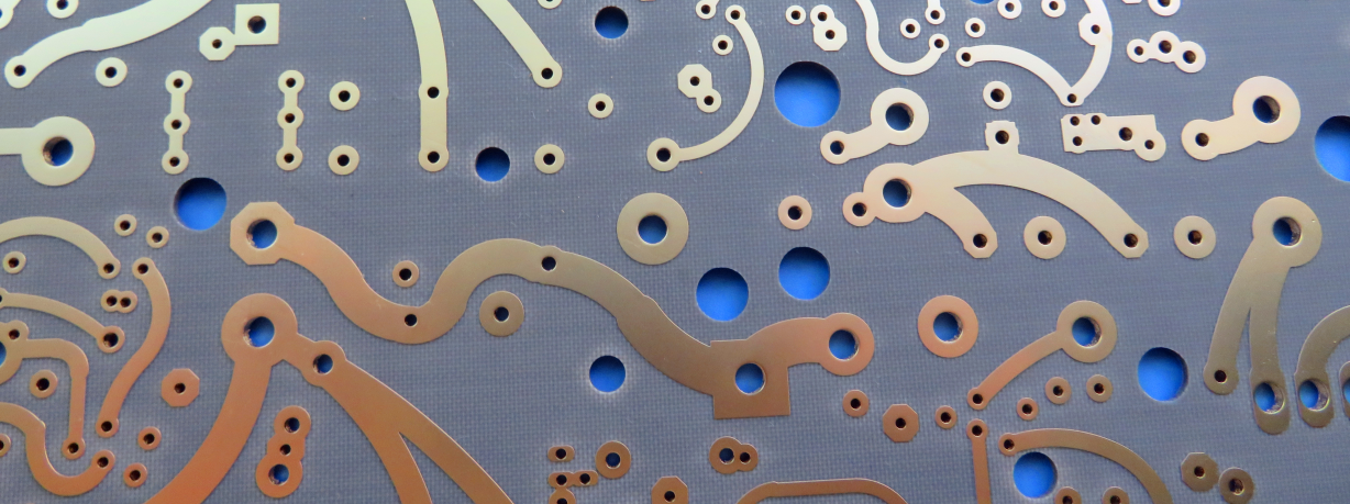
This 4-layer rigid PCB is built on Wangling F4BTMS1000 base material, meeting IPC-Class 2 quality standards. It has a finished thickness of 12.9mm, board dimensions of 145mm x 145mm (1 piece, ±0.15mm tolerance), and features 1oz (1.4 mils) finished copper weight for both inner and outer layers. Key details include HASL surface finish, white silkscreen on the top layer (no bottom silkscreen), black solder mask on the top layer (no bottom solder mask), and 100% electrical testing before shipment. F4BTMS1000 PCB supports blind vias (Top to inner layer 1) and buried vias (inner layer 2 to inner layer 3), with a minimum trace/space of 5/7 mils, minimum hole size of 1.2mm, and via plating thickness of 20μm. Artwork is supplied in Gerber RS-274-X format, and the PCB is available worldwide.

PCB Construction Details
Construction Item |
Specification |
Base Material |
F4BTMS1000 |
Layer Count |
4 layers (rigid) |
Board Dimensions |
145mm x 145mm = 1PCS, ±0.15mm |
Minimum Trace/Space |
5/7 mils |
Minimum Hole Size |
1.2mm |
Vias Type |
Blind vias (Top to inner layer 1), Buried vias (inner layer 2 to inner layer 3) |
Finished Board Thickness |
12.9mm |
Finished Cu Weight (Inner/Outer) |
1oz (1.4 mils) |
Via Plating Thickness |
20 μm |
Surface Finish |
HASL |
Top Silkscreen |
White |
Bottom Silkscreen |
No |
Top Solder Mask |
Black |
Bottom Solder Mask |
No |
Electrical Test Before Shipment |
100% |
Additional Components & Features
F4BTMS1000 PCB supports 19 components, with 77 total pads (35 thru-hole pads, 42 top SMT pads, 0 bottom SMT pads), 32 vias, and 2 nets. Its stackup includes Copper_layer_1 (35μm), F4BTMS1000 Core (6.35mm/250mil), Copper_layer_2 (35μm), Prepreg RO4450F (0.102mm/4mil), Copper_layer_3 (35μm), F4BTMS1000 Core (6.35mm/250mil), and Copper_layer_4 (35μm).
Material Advantages (F4BTMS1000)
F4BTMS1000 PCB is an upgraded version of the F4BTM series, with enhanced performance via ceramic enrichment and ultra-thin/ultra-fine glass fiber cloth reinforcement. It has a dielectric constant (Dk) of 10.2 at 10GHz, dissipation factor of 0.0020 at 10GHz (0.0023 at 20GHz), and CTE of 16 ppm/°C (x-axis), 18 ppm/°C (y-axis), 32 ppm/°C (z-axis, -55°C to 288°C). It also features low Dk thermal coefficient (-320 ppm/°C, -55°C to 150°C), high thermal conductivity (0.81 W/mk), low moisture absorption (0.03%), RTF low roughness copper foil (reduces conductor loss, ensures good peel strength), and compatibility with copper/aluminum bases. It minimizes glass fiber’s impact on electromagnetic waves, improving dimensional stability and usable frequency range.
Typical Applications
Ideal for aerospace equipment (space and cabin equipment), microwave/RF devices, radar (military radar), feed networks, phase-sensitive antennas (phased array antennas), and satellite communications.
Why Choose This PCB?
This 4-layer PCB leverages F4BTMS1000’s high reliability and performance—including low dielectric loss, stable thermal properties, and compatibility with aerospace standards—paired with precise construction (blind/buried vias, HASL finish) and 100% electrical testing. Compliance with IPC-Class 2 and worldwide availability ensure it meets diverse high-demand project needs.
Order Now for Aerospace, Microwave & Radar Applications!
4-Layer F4BTMS1000 4-layer PCB delivers the stability and performance required for aerospace equipment, microwave devices, and radar systems—order now to support your high-reliability electronic projects.