

 Home
Home
F4BM High-Frequency PCB Superior Low-Loss Substitute for Demanding RF Applications
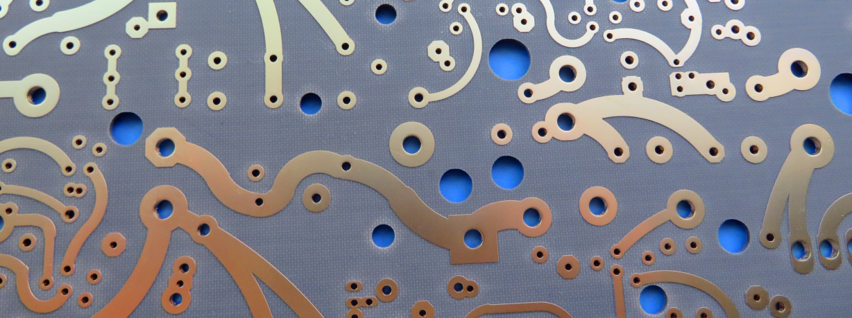
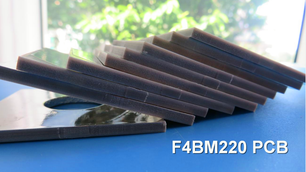
The F4BM series of high-frequency circuit board laminates are engineered by scientifically formulating and laminating a composite of fiberglass cloth
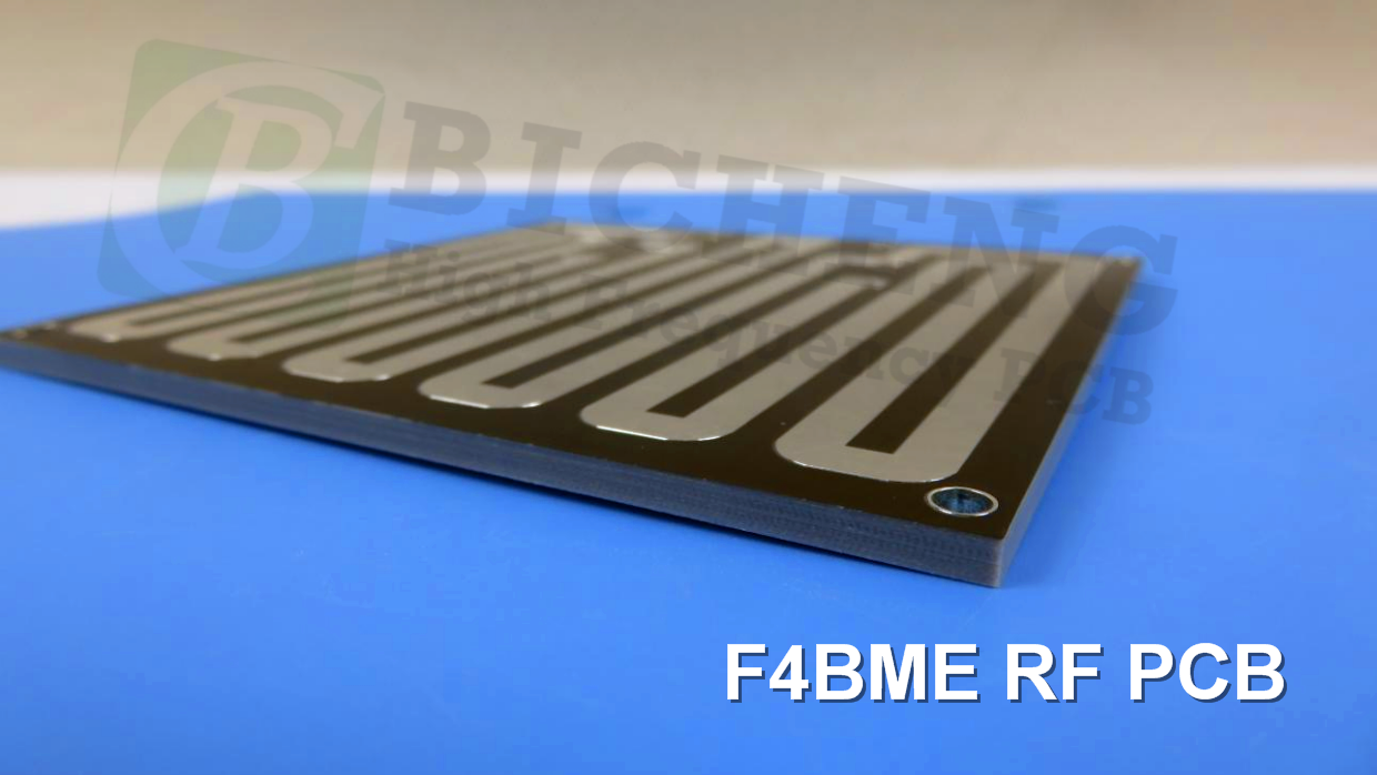
F4BME Low-Loss PTFE PCB Laminates with Controlled DK and PIM Performance
F4BME PCB is paired with reverse-treated foil (RTF) copper foil, offering excellent PIM performance, more precise line control, and lower conductor loss.
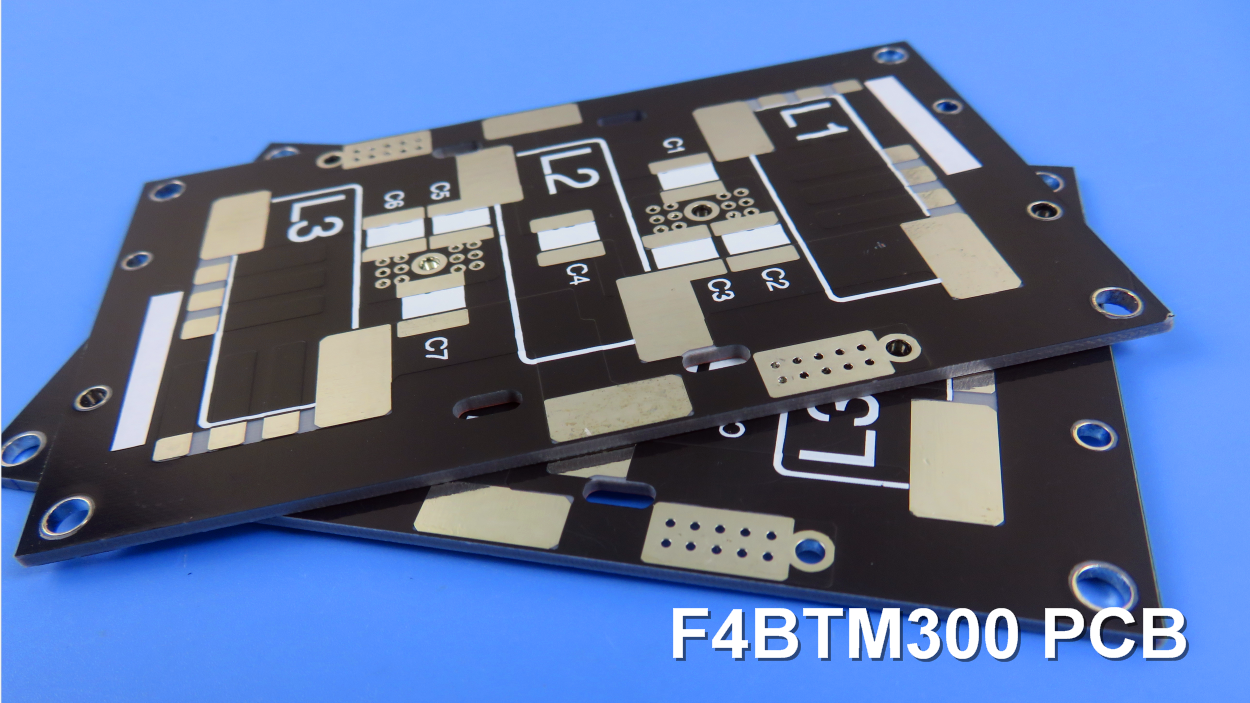
F4BTM High Frequency PCB Advanced Low Thermal Expansion Coefficient Materials for High-Performance Circuitry
Discover F4BTM series PCB, meticulously crafted by combining fiberglass cloth, nano-ceramic particles, and polytetrafluoroethylene (PTFE) resin
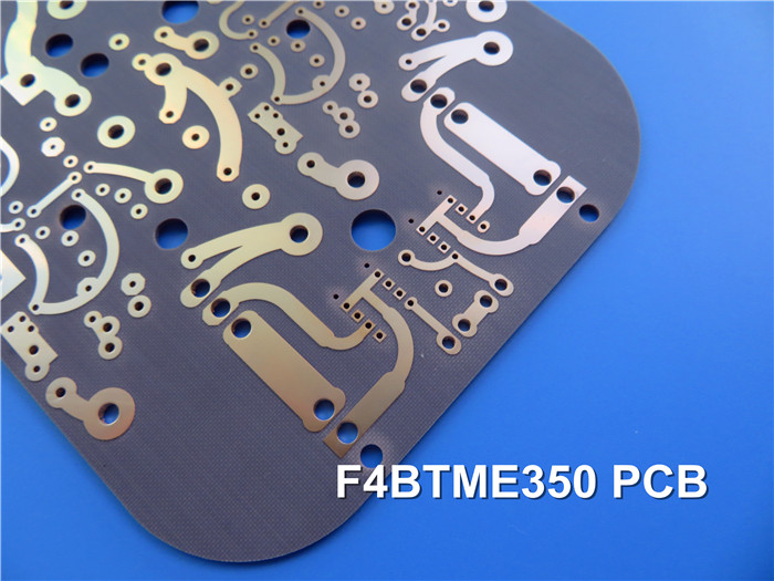
F4BTME Series PCB Engineered Low Loss Laminates with Nano-Ceramics for Low PIM
Built on the F4BM dielectric layer, the F4BTME PCB incorporates high-dielectric, low-loss nano-scale ceramics
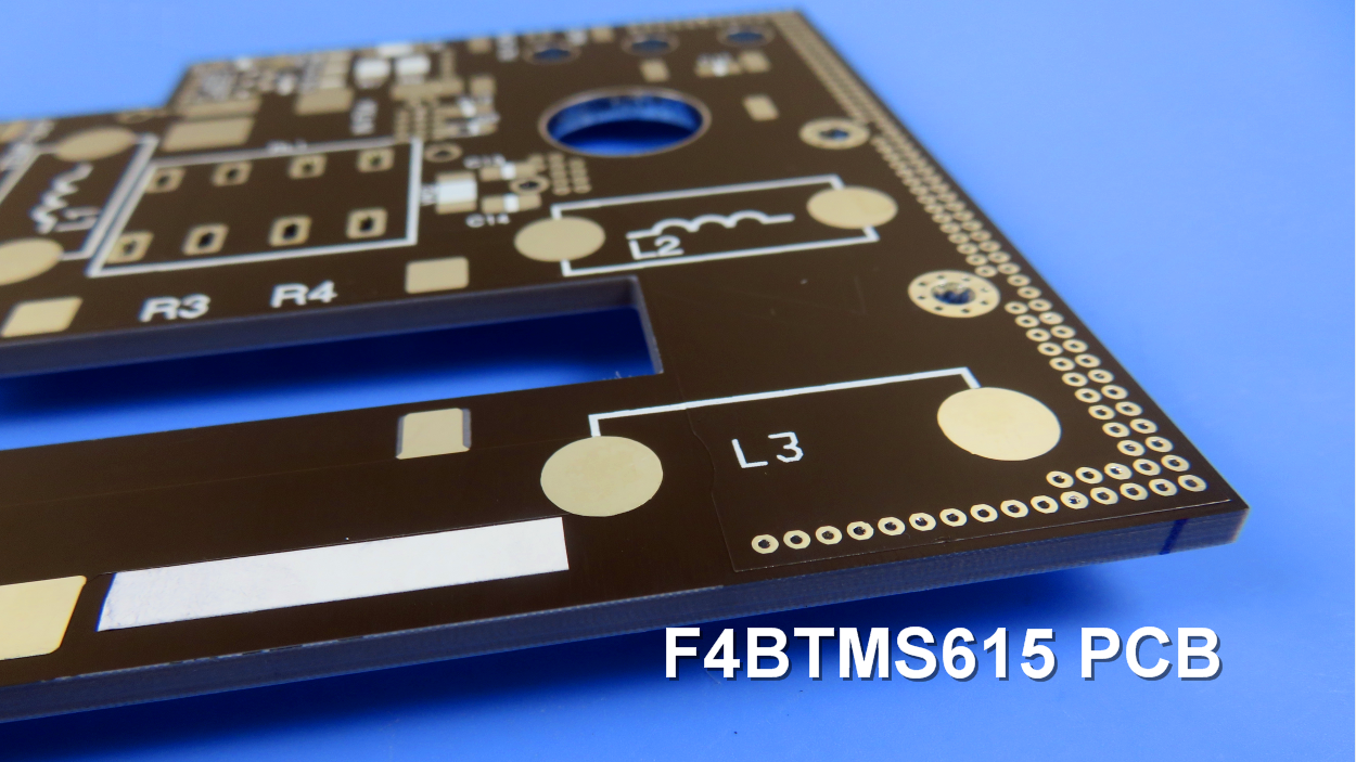
F4BTMS High-Frequency PCB: Enhanced Ceramic Composite Laminates for High-Performance Applications
The F4BTMS High-Frequency PCB is an upgraded version of the F4BTM series. Based on the foundation of the F4BTM series, it has achieved significant technological breakthroughs in material formulation and manufacturing processes.

F4BTMS1000 4-Layer 12.9mm HDI PCB with Blind Via Buried Vias for Microwave and Radar Applications
This 4-layer rigid PCB is built on Wangling F4BTMS1000 base material, meeting IPC-Class 2 quality standards.F4BTMS1000 PCB supports blind vias (Top to inner layer 1) and buried vias (inner layer 2 to inner layer 3)