

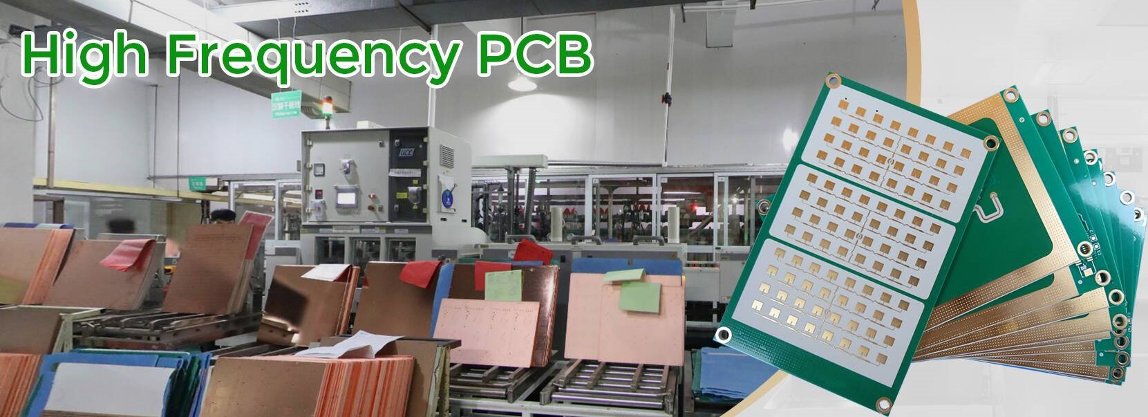
Products
 Home
Home
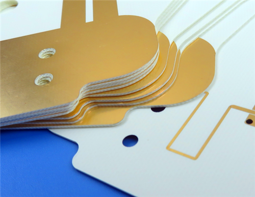
Rogers DiClad 880 High Frequency PCB 2-Layer 20mil 0.508mm Immersion Gold PCB for Digital Radio Antennas
This Rogers high - frequency PCB is constructed from DiClad 880 laminates. It features a double - layer design, with the signal layer situated on the top surface and the shielding layer on the bottom.
.jpg)
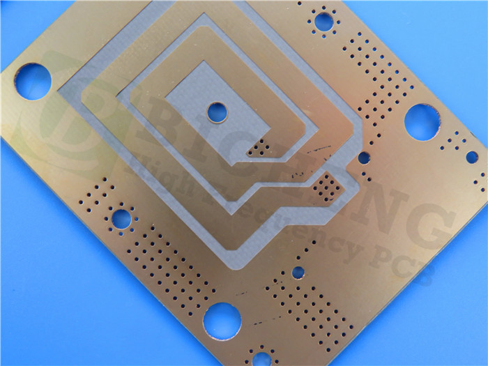
1.524mm Double Layer Rogers AD255C PCB Antenna Circuit Board for critical wireless applications with Immersion Gold
Rogers AD255C PCBs serve as the base material for this specialized antenna PCB, which features a double-layer design
.jpg)
Rogers IsoClad 917 High Frequency PCB Rogers non-woven fiberglass/PTFE PCB Materials for Antennas Application
As a non-woven fiberglass-reinforced solution, IsoClad 917 PCB is less rigid compared to woven fiberglass-based laminates.
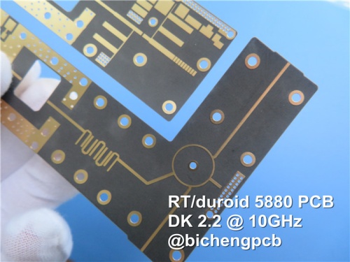
Rogers RT Duroid 5880 PTFE Composite PCB 10mil 20mil 31mil 62mil Thickness with Immersion Gold, Immersion Silver, Immersion Tin and HASL
Rogers RT/duroid 5880 PCB delivers exceptional electrical properties for demanding microwave and millimeter-wave applications, available in multiple thickness configurations
.jpg)
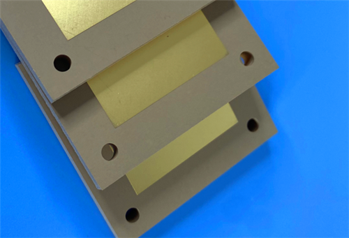
Rogers RT/duroid 6002 PCB Built on 20mil Double-layer laminate With HASL Lead Free for Ground Based and Airborne Radar Systems
Rogers RT/duroid 6002 PCB stands as a groundbreaking low-loss, low-dielectric-constant laminate that delivers exceptional electrical and mechanical properties for demanding microwave applications.
TP440 2-Layer 0.6mm High Frequency PCB with Immersion Gold Surface Finish for GPS and Miniature Antenna Applications
Wangling TP440 PCB is a premium 2-layer rigid high frequency printed circuit board built on authentic 0.5mm TP440 core material, designed for high-precision RF circuits and miniature antenna systems.
TF300 Low Loss PCB 2-Layer 0.7mm Immersion Gold Circuit Board for Phase-sensitive Antennas and Phased Array Antennas
Wangling TF300 PCB is a professional 2-layer rigid high frequency printed circuit board built on premium 0.635mm Wangling TF300 ceramic-filled PTFE core material.
TMM10 1-Layer 60mil Thermoset PCB Rogers Microwave Material with OSP for GPS Antennas and Patch Antennas
Rogers TMM10 PCB is a high-performance thermoset microwave rigid printed circuit board engineered for high-precision stripline, microstrip, and high-reliability microwave circuit applications.