

 Home
Home
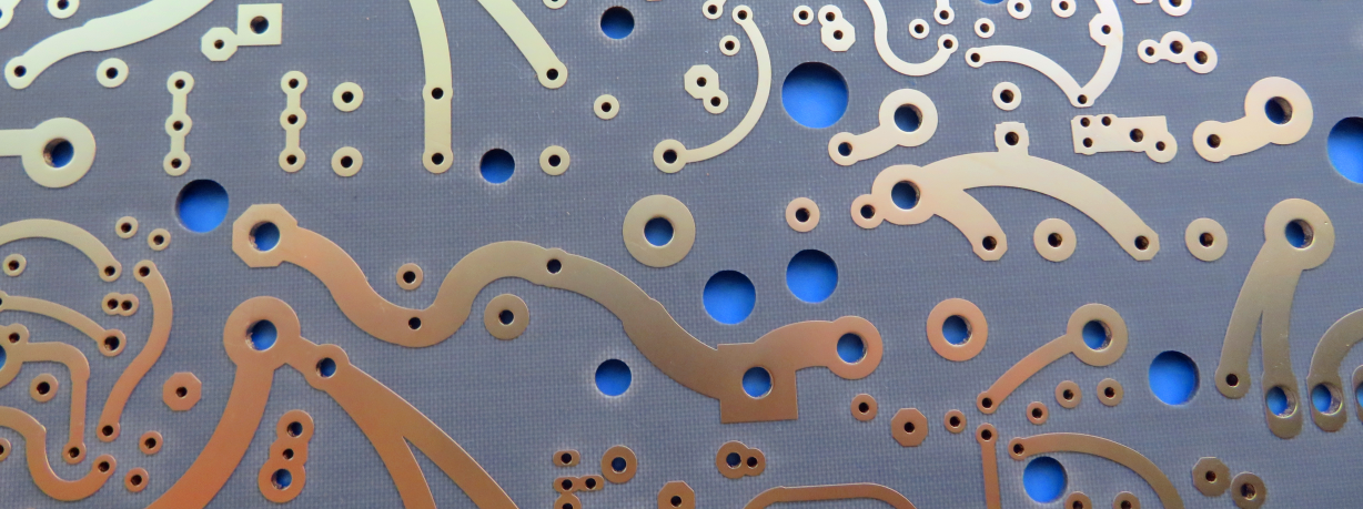
F4BTME Series PCB Engineered Low Loss Laminates with Nano-Ceramics for Low PIM
Printed Circuit Boards are custom-made products; the images and specifications provided are for reference only.
Introduction
F4BTME series PCB is manufactured through the scientific formulation of fiberglass cloth, nano-ceramic fillers, and polytetrafluoroethylene (PTFE) resin, followed by rigorous pressing processes. Built on the F4BM dielectric layer, the F4BTME PCB incorporates high-dielectric, low-loss nano-scale ceramics—this modification not only retains the material’s low-loss properties but also delivers higher dielectric constant (DK), enhanced heat resistance, lower coefficient of thermal expansion (CTE), higher insulation resistance, and improved thermal conductivity.
While F4BTM and F4BTME share the same dielectric layer, they differ in the copper foil used: F4BTM is paired with ED copper foil, making it ideal for applications that do not require Passive Intermodulation (PIM) performance. In contrast, F4BTME is equipped with reverse-treated (RTF) copper foil, which provides excellent PIM performance, more precise circuit trace control, and reduced conductor loss.
Features & Benefits
- DK range from 2.98 to 3.5 is available
- Addition of ceramics enhances the performance.
- F4BTME exhibits excellent PIM performance,
- Comes in various thicknesses and sizes, offers cost savings
- Commercialization, large-scale production, and high cost-effectiveness.
- Radiation-resistant and low out-gassing properties
Models & Data Sheet
| Product Technical Parameters | Product Models & Data Sheet | ||||||
| Product Features | Test Conditions | Unit | F4BTME298 | F4BTME300 | F4BTME320 | F4BTME350 | |
| Dielectric Constant (Typical) | 10GHz | / | 2.98 | 3.0 | 3.2 | 3.5 | |
| Dielectric Constant Tolerance | / | / | ±0.06 | ±0.06 | ±0.06 | ±0.07 | |
| Loss Tangent (Typical) | 10GHz | / | 0.0018 | 0.0018 | 0.0020 | 0.0025 | |
| 20GHz | / | 0.0023 | 0.0023 | 0.0026 | 0.0035 | ||
| Dielectric Constant Temperature Coefficient | -55 º~150ºC | PPM/℃ | -78 | -75 | -75 | -60 | |
| Peel Strength | 1 OZ F4BTM | N/mm | >1.6 | >1.6 | >1.6 | >1.6 | |
| 1 OZ F4BTME | N/mm | >1.4 | >1.4 | >1.4 | >1.4 | ||
| Volume Resistivity | Standard Condition | MΩ.cm | ≥1×10^7 | ≥1×10^7 | ≥1×10^7 | ≥1×10^7 | |
| Surface Resistivity | Standard Condition | MΩ | ≥1×10^6 | ≥1×10^6 | ≥1×10^6 | ≥1×10^6 | |
| Electrical Strength (Z direction) | 5KW,500V/s | KV/mm | >26 | >30 | >32 | >32 | |
| Breakdown Voltage (XY direction) | 5KW,500V/s | KV | >34 | >35 | >40 | >40 | |
| Coefficientof Thermal Expansion | XY direction | -55 º~288ºC | ppm/ºC | 15,16 | 15,16 | 13,15 | 10,12 |
| Z direction | -55 º~288ºC | ppm/ºC | 78 | 72 | 58 | 51 | |
| Thermal Stress | 260℃, 10s,3 times | No delamination | No delamination | No delamination | No delamination | ||
| Water Absorption | 20±2℃, 24 hours | % | ≤0.05 | ≤0.05 | ≤0.05 | ≤0.05 | |
| Density | Room Temperature | g/cm3 | 2.25 | 2.25 | 2.20 | 2.20 | |
| Long-Term Operating Temperature | High-Low Temperature Chamber | ℃ | -55~+260 | -55~+260 | -55~+260 | -55~+260 | |
| Thermal Conductivity | Z direction | W/(M.K) | 0.42 | 0.42 | 0.50 | 0.54 | |
| PIM | Only applicable to F4BTME | dBc | ≤-160 | ≤-160 | ≤-160 | ≤-160 | |
| Flammability | / | UL-94 | V-0 | V-0 | V-0 | V-0 | |
| Material Composition | / | / | PTFE, Fiberglass Cloth, nano-ceramics F4BTM paired with ED copper foil, F4BTME paired with reverse-treated (RTF) copper foil. |
||||
Our PCB Capability (F4BTM)
| PCB Capability (F4BTME) | |||
| PCB Material: | PTFE / glass fiber cloth / Nano-ceramic filler | ||
| Designation (F4BTME ) | F4BTM | DK (10GHz) | DF (10 GHz) |
| F4BTME298 | 2.98±0.06 | 0.0018 | |
| F4BTME300 | 3.0±0.06 | 0.0018 | |
| F4BTME320 | 3.2±0.06 | 0.0020 | |
| F4BTME350 | 3.5±0.07 | 0.0025 | |
| Layer count: | Single Sided, Double Sided PCB, Multilayer PCB, Hybrid PCB | ||
| Copper weight: | 0.5oz (17 µm), 1oz (35µm), 2oz (70µm) | ||
| Dielectric thickness (or overall thickness) | 0.25mm, 0.508mm, 0.762mm, 0.8mm, 1.0mm, 1.016mm, 1.27mm, 1.524mm, 2.0mm, 3.0mm, 4.0mm, 5.0mm, 6.0mm, 8.0mm, 10.0mm, 12.0mm | ||
| PCB size: | ≤400mm X 500mm | ||
| Solder mask: | Green, Black, Blue, Yellow, Red etc. | ||
| Surface finish: | Bare copper, HASL, ENIG, Immersion silver, Immersion tin, OSP, Pure gold, ENEPIG etc.. |