

 Home
-
HDI PCB
-
10-Layer High-Tg FR-4 HDI PCB with Immersion Gold Finish for High-Density PLC Modules
Home
-
HDI PCB
-
10-Layer High-Tg FR-4 HDI PCB with Immersion Gold Finish for High-Density PLC Modules
10-Layer High-Tg FR-4 HDI PCB with Immersion Gold Finish for High-Density PLC Modules
Printed Circuit Boards are custom-made products; the images and specifications provided are for reference only.
1.1 General description
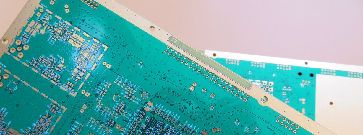
This 10-layer HDI PCB is a high-performance board designed for PLC control modules. Built on a high-Tg 170°C FR-4 substrate from Shengyi, it features a 2.0mm thickness and supports a high pin-count BGA with a fine 0.5mm pitch. The board utilizes an advanced HDI structure with blind vias (L8 to Bottom) and buried vias (L3 to L5). It is finished with Immersion Gold on pads and a green solder mask with white silkscreen, manufactured per IPC-6012 Class 2. Boards are supplied 1-up and shipped in packs of 20.
.jpg)
1.2 Features and benefits
1. High Tg industrial standard material shows excellent thermal reliability;
2. Immersion gold ensure excellent wetting during component soldering and avoid copper corrosion;
3. In house, engineering design prevents problems from occurring in pre-production;
4. ISO9001, ISO14001, IATF16949, ISO13485, UL Certified;
5. Customer complaint rate: <1%
6. Delivery on time: >98%
7. Prototype PCB capability to Volume Production capability;
8. Multilayer and Any Layer HDI PCBs;
9. More than 20+ years of PCB experience.
1.3 Applications
Converter
USB Wireless Adapter
12V Inverter
Wireless Router Reviews
Ladder Logic
Battery Inverter
CCTV Security
Wireless G Router
Programmable Controllers
Backplanes
1.4 PCB Specifications
| Item | Description | Value | ||||||||||
| Layer count | 10 Layers PCB | 10 Layers Board | ||||||||||
| Board type | Multilayer PCB | Multilayer PCB Board | ||||||||||
| Board size | 168.38 x 273.34mm=1up | 168.38 x 273.34mm=1up | ||||||||||
| Laminate | Laminate Type | FR4 | ||||||||||
| Supplier | SHENGYI | |||||||||||
| Tg | TG ≧170 | |||||||||||
| Finished thickness | 2.0+/-10% MM | |||||||||||
| Plating Thickness | PTH Cu thickness | >20 um | ||||||||||
| Inner layer Cu Thickness | 1/1 OZ | |||||||||||
| Surface Cu thickness | 35 um | |||||||||||
| Solder Mask | Material type | LP-4G G-05 | ||||||||||
| Supplier | Nan Ya | |||||||||||
| Color | Green | |||||||||||
| Single / both sides | Both Sides | |||||||||||
| S/M thickness | >=10.0 um | |||||||||||
| 3M tape test | NO Peel Off | |||||||||||
| Legend | Material type | S-380W | ||||||||||
| Supplier | Tai yo | |||||||||||
| Color | White | |||||||||||
| Location | Both Sides | |||||||||||
| 3M tape test | No peel off | |||||||||||
| Circuit | Trace Width (mm) | 0.203+/-20%mm | ||||||||||
| Spacing (mm) | 0.203+/- 20%mm | |||||||||||
| Identification | UL mark | 94V-0 | ||||||||||
| Company Logo | QM2 | |||||||||||
| Date code | 1017 | |||||||||||
| Mark location | CS | |||||||||||
| Immersion Gold | Nickel | 100u'' | ||||||||||
| Gold | ≧2u'' | |||||||||||
| Reliabilty Tests | Thermal shock test | 288±5℃, 10sec ,3 cycles | ||||||||||
| solder abllity test | 245±5℃ | |||||||||||
| Function | Electrioal Test | 233+/-5℃ | ||||||||||
| Standard | IPC-A 600H class 2, IPC_6012C CLASS 2 | 100% | ||||||||||
| Appearance | Visual inspection | 100% | ||||||||||
| warp and twist | <= 0.75% |
1.5 BGA and via plug
The full name of the BGA is Ball Grid Array, which is a type of surface mount package used for integrated circuit (IC). It has the characteristics of: ① packaging area reduced ② function increased and the number of pins increased ③ solder can be self-centered when dissolved soldering, easy to put on tin ④ reliability is high ⑤ electric performance is good and low cost etc. PCB board with BGA generally have more small holes. Mostly, via holes under BGA are designed to be 8~12mil in diameter by customers. Vias under BGA have to be plugged by resin, soldering ink is not allowed to be onto pads and no drilling on BGA pads. The plugged vias are 0.25mm, 0.3mm, 0.35mm, 0.4mm, 0.45mm, 0.5mm and 0.55mm.