

 Home
-
Newly shipped PCBs
-
Rogers TC350 and Isola FR408HR Hybrid 8-Layer PCB Resin-Filled Vias with Edge Plating
Home
-
Newly shipped PCBs
-
Rogers TC350 and Isola FR408HR Hybrid 8-Layer PCB Resin-Filled Vias with Edge Plating
Rogers TC350 and Isola FR408HR Hybrid 8-Layer PCB Resin-Filled Vias with Edge Plating
Printed Circuit Boards are custom-made products; the images and specifications provided are for reference only.
1. Rogers TC350 and Isola FR408HR Hybrid PCB
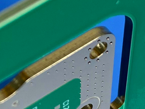
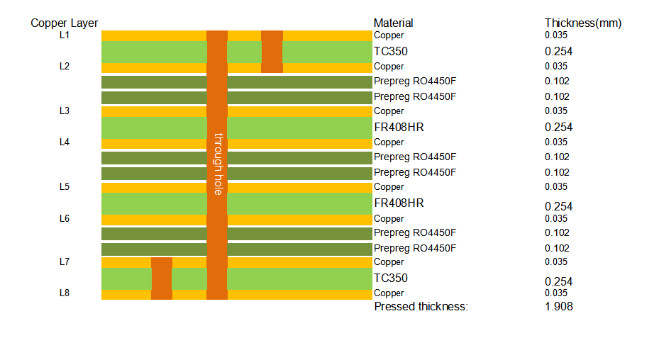
Rogers TC350 and Isola FR408HR hybrid printed circuit board is engineered for advanced high-frequency and high-speed digital applications requiring exceptional thermal management and signal integrity. This 8-layer Rogers TC350 circuit board utilizes a balanced symmetrical stackup combining 10mil TC350 ceramic-filled PTFE laminate with 10mil FR408HR high-performance FR-4 material, bonded with RO4450F prepreg and pressed to a finished thickness of 2.0mm. Each layer features 1 oz finished copper for robust current handling. The design incorporates blind vias, 0.2mm resin-filled and copper-capped vias, and full edge plating for enhanced electromagnetic shielding and environmental protection.
The complete specifications of this board are outlined in the table below.
Specification |
Details |
Layer Count |
8 Copper Layers |
Stackup Configuration |
10mil TC350 + 10mil FR408HR + 10mil FR408HR + 10mil TC350 |
Bonding Materials |
RO4450F Prepreg |
Finished Board Thickness |
2.0 mm |
Copper Weight |
1 oz (35 μm) All Layers |
Surface Finish |
ENIG (Electroless Nickel Immersion Gold) |
Solder Mask |
Green, Both Sides |
Silkscreen |
White, Both Sides |
Board Dimensions |
99 mm x 83 mm per unit |
Via Structure |
Blind Vias |
Via Filling |
0.2mm Vias, Resin Plugged and Copper Capped |
Edge Treatment |
Full Edge Plating (Metal Wrap) |
2. Understanding TC350 High-Frequency Laminate Material
2.1 Introduction to TC350
Rogers TC350 is a ceramic-filled PTFE-based woven glass reinforced composite material manufactured by Rogers Corporation, specifically designed for applications requiring a unique combination of low insertion loss and higher thermal conductivity. This material enables superior reliability and reduced operating temperatures in high power applications, making it an ideal choice for power amplifiers and RF/microwave circuits.
Rogers TC350 PCB material features a dielectric constant that remains stable across a wide frequency and temperature range, with a low thermal coefficient of dielectric constant ensuring consistent electrical performance under varying operating conditions. TC350 PCB substrate does not require special through-hole treatments needed for conventional PTFE-based materials, simplifying fabrication while maintaining excellent plated through-hole reliability.
2.2 Key Features and Properties of TC350
The TC350 material offers the following performance characteristics:
Property |
Value |
Dielectric Constant (Dk) at 10 GHz |
3.50 ± 0.05 |
Dissipation Factor (Df) at 10 GHz |
0.0020 |
Thermal Conductivity |
0.72 W/m/°K |
Thermal Coefficient of Dk |
-9 ppm/°C |
Coefficient of Thermal Expansion X-Axis |
7 ppm/°C |
Coefficient of Thermal Expansion Y-Axis |
7 ppm/°C |
Coefficient of Thermal Expansion Z-Axis |
23 ppm/°C |
Volume Resistivity |
7.4 x 10⁶ Mohm |
Surface Resistivity |
3.2 x 10⁷ Mohm |
Water Absorption |
0.05% |
Peel Strength (1 oz ED Foil) |
7.0 lb/in (1.2 N/mm) |
Density |
2.3 g/cm³ |
Flammability Rating |
UL 94 V-0 |
Lead-Free Process Compatible |
Yes |
2.3 Typical Applications for TC350
The exceptional thermal and electrical properties of TC350 make it suitable for numerous high-performance applications:
High power amplifiers requiring efficient heat dissipation
Base station infrastructure and antenna systems
RF/microwave circuits and components
Power dividers and couplers
Commercial airline broadband antennas
Point-to-point digital radio systems
Industrial heating applications
3. Understanding FR408HR High-Performance Laminate Material
3.1 Introduction to FR408HR
FR408HR is a high-performance FR-4 resin system laminate and prepreg product manufactured by Isola Group using patented high-performance multifunctional resin technology, reinforced with electrical grade E-glass fabric. This material delivers a 30% improvement in Z-axis expansion and offers 25% more electrical bandwidth with lower loss compared to competitive products in this space.
The material bridges the gap from both thermal and electrical perspectives, combining superior moisture resistance at reflow with excellent high-speed performance. FR408HR is also laser fluorescing and UV blocking for maximum compatibility with Automated Optical Inspection systems, optical positioning systems, and photo-imageable solder mask imaging.
3.2 Key Features and Properties of FR408HR
The FR408HR material offers the following performance characteristics:
Property |
Value |
Glass Transition Temperature (Tg) |
190°C |
Decomposition Temperature (Td) |
360°C |
Dielectric Constant (Dk) at 2 GHz |
3.68 |
Dissipation Factor (Df) at 2 GHz |
0.0092 |
Thermal Conductivity |
0.4 W/m/°K |
X/Y-Axis CTE Pre-Tg |
16 ppm/°C |
Z-Axis CTE Pre-Tg |
55 ppm/°C |
Z-Axis CTE Post-Tg |
230 ppm/°C |
Moisture Absorption |
0.061% |
Peel Strength (RTF Foil) |
1.14 N/mm (6.5 lb/inch) |
Time to Delamination T260 |
60 minutes |
Time to Delamination T288 |
>30 minutes |
CAF Resistance |
Yes |
Flammability Rating |
UL 94 V-0 |
Lead-Free Process Compatible |
Yes |
3.3 Product Features and Availability
R408HR is RoHS compliant and offers performance attributes including CAF resistance, lead-free assembly compatibility, 0.8 mm pitch capability, 6x 260°C reflow capability, and 6x 288°C solder float capability. Processing advantages include FR-4 process compatibility, via filling capability, and support for multiple lamination cycles. Product availability includes laminate in full size sheet or panel form with RTF copper foil types in weights from ½ to 2 oz, and prepreg available in roll or panel form with glass fabric options including E-glass, square weave glass, and mechanically spread glass.
3.4 Typical Applications for FR408HR
The exceptional thermal and electrical properties of FR408HR make it suitable for networking and communications infrastructure, aerospace and defense systems, computing storage and peripheral devices, medical industrial and instrumentation equipment, High Density Interconnect designs, high-speed digital applications, and applications with high thermal reliability requirements.
4. Understanding Via Filled and Capped Technology
4.1 What is Via Filled and Capped?
Via filled and capped, also known as resin-filled and copper-capped vias or Via-in-Pad technology, is an advanced PCB manufacturing process where via holes are completely filled with a non-conductive epoxy resin, planarized to achieve a flat surface, and then plated over with copper. This creates a smooth, flat surface suitable for component placement directly over the via.
The process involves several critical steps including drilling the via holes, plating the via walls to establish conductivity, filling the vias with epoxy resin, curing the resin, planarizing the surface to remove excess material, and finally capping with copper plating. The result is a via that is completely hidden beneath a copper pad, invisible from the board surface.
4.2 Purposes and Benefits of Via Filled and Capped
Via filled and capped technology enables Via-in-Pad design by allowing vias to be placed directly under component pads, which is essential for fine-pitch BGA and QFN packages with 0.5mm pitch and smaller. This technology prevents solder wicking by eliminating solder from flowing into via holes during assembly, thus preventing voids and insufficient solder joints. It creates planar surfaces that are perfectly flat for component mounting, critical for reliable soldering. The technology improves thermal management by creating efficient thermal paths from components into internal copper planes and enhances signal integrity by reducing parasitic inductance through elimination of dog-bone fanout traces. It enables higher routing density by freeing up surface area for additional components and routing channels while supporting multiple lamination cycles for complex HDI designs.
4.3 Quality Standards
For epoxy-filled and capped vias, quality standards require hole surface copper thickness of at least 5μm, and leveled solder pads must have depression and protrusion within 50μm. Via holes should ideally be 0.5mm or smaller for reliable filling, as larger holes may be incompletely filled. For this specific board, the 0.2mm vias are well within the optimal range for reliable resin filling and copper capping.
5. Understanding Edge Plating (Metal Wrap)
5.1 What is Edge Plating?
Edge plating, also known as metal wrap or side plating, is a specialized PCB manufacturing process where a continuous metal layer is applied along the perimeter edges of the circuit board. This technique involves plating copper around the edges, connecting the top and bottom layers and creating a conductive barrier around the board's circumference.
5.2 Purposes and Benefits of Edge Plating
Edge plating provides electromagnetic shielding by creating a more complete Faraday cage around sensitive circuits, reducing electromagnetic interference emissions and improving immunity to external interference. It enhances signal integrity by providing a continuous ground reference over the entire transmission path for demanding signals such as low-voltage differential signaling and high-speed interfaces. The technology improves thermal dissipation by providing an additional path for heat transfer from the board edges, enhancing overall thermal management when combined with heat sinks or enclosures. Edge plating also increases mechanical durability by strengthening the board edges and protecting inner layers from moisture absorption through exposed edges while improving ground continuity by extending ground planes to the board perimeter.
5.3 Design Considerations
For proper adhesion and reliability, edge plating must be assigned to a specific net, typically ground, for connectivity with external pours or same-net plane layers. A minimum clearance of 0.25mm should be maintained between edge plating and any different-net copper features.
6. PCB Construction Details
Construction Feature |
Description |
Layer Stackup Configuration |
Symmetrical 8-layer hybrid stackup: top 1 oz copper on 10mil TC350, internal layers on 10mil FR408HR cores, bottom 1 oz copper on 10mil TC350, bonded with RO4450F prepreg. Total thickness 2.0mm for rigidity and hybrid dielectric performance. |
Via Technology |
Blind vias connect outer to inner layers, reducing signal path inductance. 0.2mm vias are resin-filled and copper-capped, providing flat Via-in-Pad surfaces and preventing solder wicking. |
Surface Finish |
ENIG with 2u" gold thickness offers flat, oxidation-resistant surface for fine-pitch assembly and multiple reflows; ideal for high-frequency applications. |
7. Quality Assurance and Industry Compliance
7.1 Artwork Format
The board design utilizes Gerber RS-274-X format, the industry standard for PCB fabrication data, ensuring accurate translation of design intent to manufacturing.
7.2 Manufacturing Standard
All fabrication conforms to IPC-Class-2 requirements, the industry benchmark for dedicated service electronic products, ensuring consistent quality suitable for a wide range of commercial, industrial, and military applications.
7.3 Material Approvals
TC350 carries UL 94 V-0 flammability rating and is lead-free process compatible. FR408HR is RoHS compliant, UL recognized, and carries comprehensive material certifications for high-reliability applications.
8. Conclusion
This 8-layer hybrid PCB combining Rogers TC350 ceramic-filled PTFE laminate with Isola FR408HR high-performance FR-4 material delivers exceptional performance for demanding RF/microwave and high-speed digital applications. The TC350 outer layers provide a dielectric constant of 3.50 with dissipation factor of 0.0020 at 10 GHz and thermal conductivity of 0.72 W/m/°K, ensuring minimal signal loss and efficient heat dissipation for high-power circuits. The FR408HR inner cores offer a Tg of 190°C, Td of 360°C, and Dk of 3.68 with Df of 0.0092, delivering 30% improvement in Z-axis expansion and 25% more electrical bandwidth compared to standard materials. The 2.0mm finished thickness with 1 oz copper on all layers provides robust current handling capability, while the ENIG surface finish ensures excellent solderability and long-term reliability. Blind via technology combined with resin-filled and copper-capped 0.2mm vias enables Via-in-Pad designs for fine-pitch components with planar surfaces, and full edge plating provides comprehensive EMI shielding, enhanced signal integrity, and improved thermal dissipation. With IPC-Class-2 compliance and advanced material properties, this board meets the rigorous demands of aerospace, defense, networking infrastructure, and high-reliability industrial applications worldwide.
Founded in 2003, Shenzhen Bicheng Electronics Technology Co., Ltd is an established high frequency PCB supplier and exporter in Shenzhen, China, serving customers worldwide.
We are devoted to delivering high-frequency PCB products and solutions of the highest quality, along with customized service. Get in touch with us to start your project !
Visit https://www.bicheng-enterprise.com to learn more.