

 Home
-
Newly shipped PCBs
-
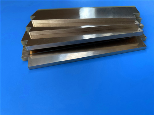
Isola I-Tera MT40 Hybrid 6-Layer PCB 50 Ohm Controlled Impedance with Edge Plating
Home
-
Newly shipped PCBs
-
Isola I-Tera MT40 Hybrid 6-Layer PCB 50 Ohm Controlled Impedance with Edge Plating
Isola I-Tera MT40 Hybrid 6-Layer PCB 50 Ohm Controlled Impedance with Edge Plating
Printed Circuit Boards are custom-made products; the images and specifications provided are for reference only.
1. Introduction
The Isola I-Tera MT40 and RO4450F prepreg hybrid printed circuit board is engineered for advanced high-speed digital and RF/microwave applications requiring exceptional signal integrity and thermal reliability. This 6-layer board utilizes I-Tera MT40 ultra-low loss laminate combined with RO4450F prepreg materials, pressed to a finished thickness of 1.501mm. The design incorporates blind vias, resin-filled and copper-capped vias, precise 50 ohm single-ended impedance control on the top layer, and full edge plating for enhanced electromagnetic shielding.
The complete specifications of this board are outlined in the table below.
Specification |
Details |
Layer Count |
6 Layers |
Base Materials |
I-Tera MT40 + RO4450F Prepreg |
Finished Board Thickness |
1.501 mm |
Inner Layer Copper Weight |
1 oz (35 μm) |
Outer Layer Copper Weight |
2 oz (70 μm) |
Surface Finish |
ENIG (Electroless Nickel Immersion Gold), 2u" Gold Thickness |
Solder Mask |
Green, Both Sides |
Silkscreen |
White, Both Sides |
Board Dimensions |
99 mm x 99 mm per unit |
Impedance Control |
50 ohm Single-Ended, Top Layer, 5 mil trace |
Via Structure |
Blind Vias |
Via Filling |
0.3mm Vias, Resin Plugged and Copper Capped |
Edge Treatment |
Full Edge Plating (Metal Wrap) |
2. Understanding I-Tera MT40 High-Performance Laminate Material
2.1 Introduction to I-Tera MT40
I-Tera MT40 is an advanced ultra-low loss laminate and prepreg material manufactured by Isola Group, specifically formulated for high-speed digital and RF/microwave printed circuit designs. This material features a dielectric constant that remains stable between -55°C and +125°C up to W-band frequencies, ensuring consistent electrical performance across extreme operating conditions.
With a dissipation factor of only 0.0031, I-Tera MT40 offers a cost-effective alternative to PTFE and other commercial microwave laminate materials while providing the processing advantages of standard FR-4 compatible manufacturing. The material does not require any special through-hole treatments commonly needed when processing PTFE-based laminates, significantly simplifying fabrication and reducing costs.
I-Tera MT40 is available in both laminate and prepreg form in typical thicknesses and standard panel sizes, providing a complete material solution package for high-speed digital multilayer, hybrid, RF/microwave, and double-sided printed circuit designs.
2.2 Key Features and Properties of I-Tera MT40
The I-Tera MT40 material offers the following performance characteristics:
Property |
Value |
Glass Transition Temperature (Tg) |
215°C |
Decomposition Temperature (Td) |
360°C |
Dielectric Constant (Dk) at 10 GHz |
3.45 |
Dissipation Factor (Df) at 10 GHz |
0.0031 |
Thermal Conductivity |
0.61 W/m/°K |
X/Y-Axis CTE Pre-Tg |
12 ppm/°C |
Z-Axis CTE Pre-Tg |
55 ppm/°C |
Z-Axis CTE Post-Tg |
290 ppm/°C |
Moisture Absorption |
0.1% |
Peel Strength (1 oz foil) |
1.0 N/mm |
Flammability Rating |
UL 94 V-0 |
Lead-Free Process Compatible |
Yes |
CAF Resistant |
Yes |
FR-4 Process Compatible |
Yes |
2.3 Typical Applications for I-Tera MT40
The exceptional electrical and thermal properties of I-Tera MT40 make it suitable for numerous high-performance applications:
Aerospace and defense systems requiring high reliability
Automotive and transportation electronics
Networking and communications infrastructure
Computing, storage, and peripheral devices
Medical, industrial, and instrumentation equipment
RF/microwave circuits and millimeter wave systems
High-speed digital designs with strict signal integrity requirements
3. Understanding Single-Ended Impedance Control
3.1 What is Single-Ended Impedance Control?
Single-ended impedance control refers to the management of the characteristic impedance of a PCB transmission line formed by a single trace and its associated reference ground plane. This impedance is a measure of the opposition to current passing through the trace at high frequencies and is essential for maintaining signal integrity by preventing reflections and signal distortion.
For single-ended signals, such as those found in clock lines, DAC/ADC interfaces, and parallel RGB LCD or camera interfaces, the trace impedance must be precisely controlled to match the driver and receiver impedances. The most common single-ended impedance value is 50 ohms, which provides an optimal balance between power handling capability and signal loss for most high-frequency applications.
3.2 Factors Affecting Single-Ended Impedance
The characteristic impedance of a single-ended trace is determined by several physical parameters:
Trace width: Increasing trace width decreases impedance
Trace thickness (copper weight): Increased copper thickness decreases impedance
Dielectric thickness: Increasing dielectric thickness increases impedance
Dielectric constant (Dk): Lower Dk materials generally result in higher impedance
Distance to reference plane: Greater distance increases impedance
Trace configuration: Microstrip (outer layer) vs. stripline (inner layer) configurations yield different impedance values for the same dimensions
For this specific board, the top layer features 5 mil traces precisely engineered to achieve 50 ohm single-ended impedance, ensuring optimal signal transmission for high-speed digital and RF circuits.
3.3 Manufacturing and Testing
Achieving accurate impedance control requires close collaboration between designers and manufacturers. The manufacturer performs testing using Time Domain Reflectometry (TDR) on dedicated test coupons to verify that the desired impedance is achieved within specified tolerances. Based on initial test results, adjustments are made to trace widths or dielectric thickness to meet the target impedance requirements.
4. Understanding Edge Plating (Metal Wrap)
4.1 What is Edge Plating?
Edge plating, also known as metal wrap or side plating, is a specialized PCB manufacturing process where a continuous metal layer is applied along the perimeter edges of the circuit board. This technique involves plating copper around the edges, connecting the top and bottom layers and creating a conductive barrier around the board's circumference.
4.2 Purposes and Benefits of Edge Plating
Edge plating serves multiple critical functions in high-performance PCB designs:
Electromagnetic shielding: Creates a more complete Faraday cage around sensitive circuits, reducing electromagnetic interference (EMI) emissions and improving immunity to external interference
Moisture protection: Prevents innerlayers from absorbing moisture through the exposed edges of the board
Thermal dissipation: Provides an additional path for heat transfer from the board edges
Mechanical durability: Enhances the mechanical strength of the board edges
Ground continuity: Extends ground planes to the board perimeter, improving overall grounding effectiveness
4.3 Edge Plating Process
The edge plating process involves several key steps:
PCB pretreatment including cleaning and micro-etching to ensure proper adhesion
Metal layer deposition through electroplating or electroless plating methods
Precise control of metal thickness, typically between 5-50 micrometers depending on application requirements
Final inspection and testing to verify continuity and adhesion quality
For this board, full edge plating provides comprehensive EMI shielding and environmental protection, essential for sensitive RF/microwave and high-speed digital applications.
5. PCB Construction Details
5.1 Layer Stackup Configuration
This 6-layer board employs a sophisticated stackup designed for optimal high-frequency performance and signal integrity. The construction utilizes I-Tera MT40 laminate combined with RO4450F prepreg bonding layers. Inner layers feature 1 oz copper for power distribution and signal routing, while outer layers incorporate heavier 2 oz copper for improved current handling and thermal dissipation.
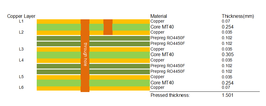
5.2 Via Technology
The board incorporates several advanced via structures to maximize routing density and signal integrity:
Blind vias connect selected outer layers to specific inner layers, reducing signal path length and minimizing parasitic inductance
0.3mm vias are resin plugged and copper capped, creating flat, planar surfaces suitable for component placement and preventing solder wicking during assembly
The resin plugging process fills via voids completely, followed by copper plating to cap and planarize the surface
5.3 Surface Finish: ENIG
Electroless Nickel Immersion Gold with 2u" gold thickness provides a flat, oxidation-resistant surface suitable for fine-pitch component assembly and multiple reflow cycles. The nickel layer offers a robust barrier against copper migration, while the gold coating ensures excellent solderability and long shelf life.
6. Quality Assurance and Industry Compliance
6.1 Artwork Format
The board design utilizes Gerber RS-274-X format, the industry standard for PCB fabrication data, ensuring accurate translation of design intent to manufacturing.
6.2 Manufacturing Standard
All fabrication conforms to IPC-Class-2 requirements, the industry benchmark for dedicated service electronic products, ensuring consistent quality suitable for a wide range of commercial, industrial, and military applications.
6.3 Material Approvals
I-Tera MT40 carries UL recognition (File Number E41625) and is RoHS compliant, ensuring compatibility with global regulatory requirements.
7. I-Tera MT40 Data sheets
I-Tera® MT40 |
||||
Property |
Typical Value |
Units |
Test Method |
|
|
|
Metric (English) |
IPC-TM-650 (or as noted) |
|
Glass Transition Temperature (Tg) by DSC |
215 |
°C |
2.4.25C |
|
Glass Transition Temperature (Tg) by DMA |
230 |
°C |
2.4.24.4 |
|
Glass Transition Temperature (Tg) by TMA |
210 |
°C |
2.4.24C |
|
Decomposition Temperature (Td) by TGA @ 5% weight loss |
360 |
°C |
2.4.24.6 |
|
Time to Delaminate by TMA (Copper removed) |
A. T260 |
>60 |
Minutes |
2.4.24.1 |
|
B. T288 |
|
|
|
Z-Axis CTE |
A. Pre-Tg |
55 |
ppm/°C |
2.4.24C |
|
B. Post-Tg |
290 |
ppm/°C |
|
|
C. 50 to 260°C, (Total Expansion) |
2.8 |
% |
|
X/Y-Axis CTE |
Pre-Tg |
12 |
ppm/°C |
2.4.24C |
Thermal Conductivity |
0.61 |
W/m·K |
ASTM E1952 |
|
Thermal Stress 10 sec @ 288ºC (550.4ºF) |
A. Unetched |
Pass |
Pass Visual |
2.4.13.1 |
|
B. Etched |
|
|
|
Dk, Permittivity |
A. @ 2 GHz |
3.45 |
— |
2.5.5.5 |
|
B. @ 5 GHz |
|
|
|
|
C. @ 10 GHz |
|
|
|
Df, Loss Tangent |
A. @ 2 GHz |
0.0031 |
— |
Bereskin Stripline |
|
B. @ 5 GHz |
|
|
|
|
C. @ 10 GHz |
|
|
|
Volume Resistivity |
C-96/35/90 |
1.33 x 10^7 |
MΩ-cm |
2.5.17.1 |
Surface Resistivity |
C-96/35/90 |
1.33 x 10^5 |
MΩ |
2.5.17.1 |
Dielectric Breakdown |
45.4 |
kV |
2.5.6B |
|
Arc Resistance |
139 |
Seconds |
2.5.1B |
|
Electric Strength (Laminate & laminated prepreg) |
45 (1133) |
kV/mm (V/mil) |
2.5.6.2A |
|
Comparative Tracking Index (CTI) |
3 |
Class (Volts) |
UL 746A |
|
|
|
|
ASTM D3638 |
|
Peel Strength |
1 oz. EDC foil |
1.0 (5.7) |
N/mm (lb/inch) |
2.4.8C |
Flexural Strength |
A. Length direction |
490 (71.0) |
MPa (kpsi) |
2.4.4B |
|
B. Cross direction |
400 (58.0) |
|
|
Tensile Strength |
A. Length direction |
269 (39.0) |
MPa (kpsi) |
ASTM D3039 |
|
B. Cross direction |
241 (35.0) |
|
|
Young's Modulus |
A. Length direction |
3060 |
ksi |
ASTM D790-15e2 |
|
B. Cross direction |
2784 |
|
|
Poisson's Ratio |
A. Length direction |
0.234 |
— |
ASTM D3039 |
|
B. Cross direction |
0.222 |
|
|
Moisture Absorption |
0.1 |
% |
2.6.2.1A |
|
Flammability (Laminate & laminated prepreg) |
V-0 |
Rating |
UL 94 |
|
Relative Thermal Index (RTI) |
130 |
°C |
UL 796 |
|
8. Conclusion
This 6-layer hybrid PCB combining Isola I-Tera MT40 ultra-low loss laminate with RO4450F prepreg delivers exceptional performance for high-speed digital and RF/microwave applications through its stable dielectric constant of 3.45 and dissipation factor of 0.0031 at 10 GHz, ensuring minimal signal loss across a broad frequency and temperature range. 1.501mm Isola I-Tera MT40 PCB with 1 oz inner copper and 2 oz outer copper provides robust current handling capability, while the ENIG surface finish ensures excellent solderability and long-term reliability. Precision 50 ohm single-ended impedance control on the top layer with 5 mil traces guarantees optimal signal integrity, and the blind via technology combined with resin-plugged and copper-capped 0.3mm vias enables high-density routing with planar surfaces. Full edge plating provides comprehensive EMI shielding and environmental protection. With Tg of 215°C, Td of 360°C, and IPC-Class-2 compliance, this board meets the rigorous demands of aerospace, defense, networking, and high-speed digital applications worldwide.
Founded in 2003, Shenzhen Bicheng Electronics Technology Co., Ltd is an established high frequency PCB supplier and exporter in Shenzhen, China, serving customers worldwide.
We are devoted to delivering high-frequency PCB products and solutions of the highest quality, along with customized service. Get in touch with us to start your project !
Visit https://www.bicheng-enterprise.com to learn more.