

 Home
-
Newly shipped PCBs
-
Rogers RT/duroid 5880 and High Tg FR4 PCB 1.0mm Ultra-Thin 4-Layer Hybrid PCB for Military Radar and Airborne Antennas
Home
-
Newly shipped PCBs
-
Rogers RT/duroid 5880 and High Tg FR4 PCB 1.0mm Ultra-Thin 4-Layer Hybrid PCB for Military Radar and Airborne Antennas
Rogers RT/duroid 5880 and High Tg FR4 PCB 1.0mm Ultra-Thin 4-Layer Hybrid PCB for Military Radar and Airborne Antennas
Printed Circuit Boards are custom-made products; the images and specifications provided are for reference only.
1. Product Introduction
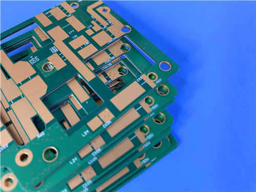
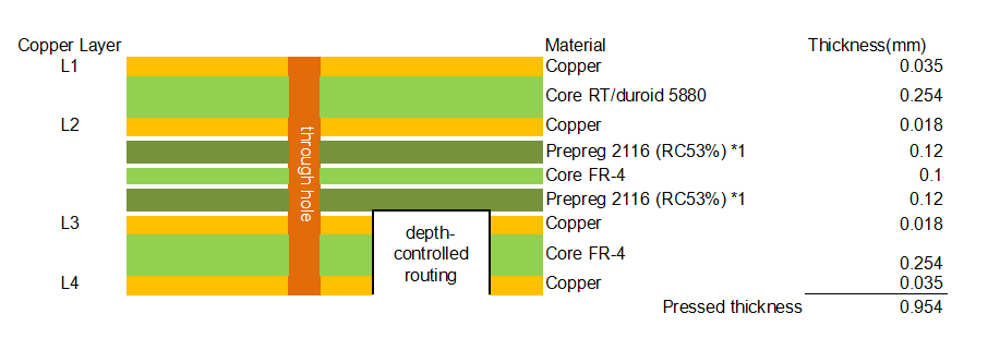
This 4-layer PCB (6-layer stackup construction) uses a hybrid combination of RT/duroid 5880 glass microfiber reinforced PTFE composite and high Tg FR4. The finished board thickness is 1.0 mm, and the panel size is 90 mm × 80 mm (1 piece per panel). Inner layer copper starts at 0.5 OZ, with finished outer copper of 1 OZ. The board features blue solder mask, white silkscreen, and immersion gold finish of 2 microinches. Additional specifications include a plated hole copper thickness of 25 µm meeting IPC Class 3 standards, and a controlled depth routing (controlled depth slot) feature.
2. Product Specification Table
Parameter |
Value / Description |
Layer count |
4 layers (6-layer stackup construction) |
Material |
RT/duroid 5880 + High Tg FR4 hybrid stackup |
Finished board thickness |
1.0 mm |
Board dimensions |
90 mm × 80 mm (1 piece) |
Inner layer copper (starting) |
0.5 OZ |
Finished outer copper |
1 OZ |
Solder mask |
Blue |
Silkscreen |
White |
Surface finish |
Immersion Gold (2 microinches) |
Plated hole copper thickness |
25 µm |
IPC standard |
Class 3 (IPC-3) |
Special feature |
Controlled depth routing (slot) |
Controlled depth routing allows precise cavities or partial slots for component recessing, shielding, or impedance control. The 25 µm hole copper thickness ensures reliable plated through-holes. Immersion gold provides a flat, solderable, oxidation-resistant surface.
3. RT/duroid 5880 Laminate Introduction
RT/duroid® 5870 and 5880 are glass microfiber reinforced PTFE composites designed for exacting stripline and microstrip circuit applications. The randomly oriented microfibers result in exceptional dielectric constant uniformity. The dielectric constant of RT/duroid 5880 laminates is uniform from panel to panel and remains constant over a wide frequency range. Its low dissipation factor extends the usefulness of RT/duroid 5880 laminates to Ku-band and above. The material is normally supplied as a laminate with electrodeposited copper of ½ to 2 ounces per square foot (8 to 70 µm) or reverse treated ED copper on both sides. For more critical electrical applications, rolled copper foil cladding is available. Aluminum, copper, or brass plate cladding may also be specified.
4.Typical Properties of RT/duroid 5880
Property |
RT/duroid 5870 Typical Values |
RT/duroid 5880 Typical Values |
Direction |
Units |
Condition |
Test Method |
Dielectric Constant, εr (Process) |
2.332.33 ± 0.02 spec. |
2.202.20 ± 0.02 spec. |
Z |
N/A |
C24/23/50 |
1 MHz: IPC-TM-650 2.5.5.310 GHz: IPC-TM 2.5.5.5 |
Dielectric Constant, εr (Design) |
2.33 |
2.20 |
Z |
N/A |
8 GHz – 40 GHz |
Differential Phase Length Method |
Dissipation Factor, tan δ |
0.00050.0012 |
0.00040.0009 |
Z |
N/A |
C24/23/50 |
1 MHz: IPC-TM-650 2.5.5.310 GHz: IPC-TM 2.5.5.5 |
Thermal Coefficient of εr |
-115 |
-125 |
Z |
ppm/°C |
-50 – 150°C |
IPC-TM-650 2.5.5.5 |
Volume Resistivity |
2 × 10⁷ |
2 × 10⁷ |
Z |
Mohm·cm |
C96/35/90 |
ASTM D257 |
Surface Resistivity |
2 × 10⁷ |
3 × 10⁷ |
Z |
Mohm |
C/96/35/90 |
ASTM D257 |
Specific Heat |
0.96 (0.23) |
0.96 (0.23) |
N/A |
J/g/K (cal/g/°C) |
N/A |
Calculated |
Tensile Modulus @23°C |
1300 (189) X1280 (185) Y |
1070 (156) X860 (125) Y |
X,Y |
MPa (kpsi) |
Condition A |
ASTM D638 |
Tensile Modulus @100°C |
490 (71) X430 (63) Y |
450 (65) X380 (55) Y |
X,Y |
MPa (kpsi) |
Condition A |
ASTM D638 |
Tensile Ultimate Stress |
50 (7.3) X42 (6.1) Y |
29 (4.2) X27 (3.9) Y |
X,Y |
MPa (ksi) |
- |
ASTM D638 |
Tensile Ultimate Strain |
9.8 X9.8 Y |
6.0 X4.9 Y |
X,Y |
% |
- |
ASTM D638 |
Compressive Modulus |
1210 (176) X1360 (198) Y803 (120) Z |
710 (103) X710 (103) Y940 (136) Z |
X,Y,Z |
MPa (kpsi) |
Condition A |
ASTM D695 |
Compressive Ultimate Stress |
30 (4.4) X37 (5.3) Y54 (7.8) Z |
27 (3.9) X29 (5.3) Y52 (7.5) Z |
X,Y,Z |
MPa (ksi) |
- |
ASTM D695 |
Compressive Ultimate Strain |
4.0 X3.3 Y8.7 Z |
8.5 X7.7 Y12.5 Z |
X,Y,Z |
% |
- |
ASTM D695 |
Moisture Absorption |
0.02 |
0.02 |
N/A |
% |
0.062” (1.6mm), D48/50 |
ASTM D570 |
Thermal Conductivity |
0.22 |
0.20 |
Z |
W/m/K |
80°C |
ASTM C518 |
Coefficient of Thermal Expansion |
22 X28 Y173 Z |
31 X48 Y237 Z |
X,Y,Z |
ppm/°C |
0–100°C |
IPC-TM-650 2.4.41 |
Td |
500 |
500 |
N/A |
°C (TGA) |
N/A |
ASTM D3850 |
Density |
2.2 |
2.2 |
N/A |
g/cm³ |
N/A |
ASTM D792 |
Copper Peel Strength |
27.2 (4.8) |
31.2 (5.5) |
N/A |
pli (N/mm) |
1 oz (35μm) EDC foil, after solder float |
IPC-TM-650 2.4.8 |
Flammability |
V-0 |
V-0 |
N/A |
N/A |
N/A |
UL94 |
Lead-Free Process Compatible |
Yes |
Yes |
N/A |
N/A |
N/A |
N/A |
5. Typical Applications of RT/duroid 5880
Commercial airline broadband antennas, microstrip and stripline circuits, millimeter wave applications, military radar systems, missile guidance systems, and point-to-point digital radio antennas.
6.Fabrication Guidelines for RT/duroid 5880
RT/duroid 5880 laminates are shipped in reinforced corrugated cardboard containers with protective sheets. Upon receipt, inspect immediately and report any damage to the carrier and to Rogers' Customer Service within 30 days. Each panel is labeled with product, lot, and sheet numbers; maintain this traceability through storage and processing. Store at normal room temperature (65–85°F / 18–30°C) and humidity. Keep panels sealed in their original polyethylene bags or with adherent sheets to prevent copper oxidation. Stack cartons flat, maximum five high. For panels removed from cartons, store on edge in slotted shelving with clad surfaces vertical; if horizontal storage is necessary, use a flat, clean shelf with soft separator sheets and keep loading below 50 lbs/ft².
PTFE materials are softer than standard laminates. Always wear knit nylon or non-absorbent gloves when handling to prevent fingerprint corrosion. If fingerprints occur, remove by bright dipping in dilute hydrochloric acid, degreasing with acetone or MEK, water rinsing, baking at 250°F (125°C) for 60 minutes, then repeating the bright dip. Keep work surfaces clean and dry. Leave protective polyethylene sheets on during shearing, sawing, or punching. Pick panels by two edges only – thin cores lack stiffness and can be permanently creased if handled by one edge. Transport panels on flat carrying trays, interleaved with soft, sulfur-free paper.
To remove the self-adhering polyethylene sheet, lay the panel flat, peel back a corner and extend across the short edge, then gently peel horizontally. Remove adhesive residue with a lint-free cloth soaked in isopropanol (70–100%), then rinse with clean water. Remove copper oxides using commercial cleaners and microetchants. Abrasive cleaning (pumice or brush scrubbing) is not recommended because it creates microscopic scratches that can lead to thermal stress cracks; if unavoidable, use minimal pressure.
For drilling, avoid smear – PTFE smear cannot be removed, so it must be prevented by tight process control. Use carbide drills with standard geometry and 130° lip angle. Undercut drills may help reduce re-deposited debris. Always use new or precision-repointed drills. Recommended parameters: surface speed 150–250 SFM (45–75 m/min), infeed 0.0015–0.0025 inch per revolution, retract rate 400–500 IPM (10–13 m/min). Stack height (including entry/exit materials) should not exceed 75% of the drill flute length, typically less than 0.240 inch (6.1 mm). Use phenolic composite entry (0.010–0.030") and exit (>0.060"). Tool life: for a stack height of 0.060" (1.5 mm), maximum 300 hits; for 0.120" (3.0 mm), 250 hits; for 0.180" (4.5 mm), 100 hits. After drilling, remove loose debris using vapor or hydro-honing with adequate support of the soft laminate.
Before metallization, drilled holes in PTFE require surface activation. Sodium treatment is the preferred method for RT/duroid 5880. Plasma treatment should only be considered if a direct metallization process (instead of electroless copper) is used. Without such treatment, poor metal adhesion or plating voids will occur.
7.What Is Controlled Depth Routing?
Controlled depth routing, also known as controlled depth slotting or back-milling, is a machining process that creates cavities, slots, or recesses that do not go through the entire board thickness. This feature allows components to be embedded within the board for improved thermal management, reduced signal path length, or shielding. In this PCB, the controlled depth routing is implemented precisely to meet design requirements without compromising the integrity of the hybrid stackup.
8.High-Frequency Hybrid PCB with PTFE and FR4
This board combines RT/duroid 5880 (a low-loss PTFE composite) with high Tg FR4. Such a hybrid construction is used when a circuit requires superior high-frequency performance on certain layers (e.g., RF or microwave signals) while other layers can use standard FR4 for power distribution, grounding, or lower-speed signals. The PTFE layer provides excellent dielectric stability and low loss up to Ku-band and beyond, while FR4 adds mechanical rigidity and cost efficiency.
9.Advantages of Hybrid PTFE+FR4 Construction
The hybrid design delivers exceptional high-frequency performance on critical RF paths due to RT/duroid 5880's uniform Dk and low dissipation factor. Cost is reduced by limiting expensive PTFE material to only the necessary layers. The board maintains good dimensional stability and can be machined using standard methods (cutting, shearing, routing) as PTFE composites are not brittle. Additionally, the combination allows for controlled impedance and minimal signal distortion in broadband and millimeter-wave circuits.
10.Disadvantages and Considerations
PTFE-based materials like RT/duroid 5880 require specialised via preparation (sodium or plasma treatment) before electroless copper deposition, unlike standard FR-4 or hydrocarbon laminates. Hybrid lamination with FR4 demands careful control of temperature and pressure due to different coefficients of thermal expansion. The material is softer than FR4, which can lead to burring or creasing if handling and drilling are not optimised. Abrasive cleaning is discouraged. Overall, fabrication costs are higher than all-FR4 boards, and not all PCB manufacturers are experienced with PTFE hybrid stacks.
11.Summary
Rogers RT/duroid 5880 4-layer PCB uses a hybrid stackup of RT/duroid 5880 and high Tg FR4 with a finished thickness of 1.0 mm and dimensions of 90 mm × 80 mm. It features 0.5 OZ inner copper, 1 OZ finished outer copper, blue solder mask, white silkscreen, and immersion gold (2 microinches). Hole copper thickness is 25 µm, meeting IPC Class 3. A controlled depth routing feature is included. The RT/duroid 5880 laminate enables low-loss, uniform Dk performance up to Ku-band. Key fabrication guidelines: store at room temperature, handle with gloves, avoid abrasive cleaning, use carbide drills with 150–250 SFM and strict tool life limits (e.g., 300 hits at 0.060" stack height), and perform sodium treatment on drilled holes before metallisation to ensure plating reliability.