

 Home
-
Newly shipped PCBs
-
Rogers RO4350B and FR4 Tg180 Hybrid PCB – 1.553mm 8-Layer PCB with Blind and Buried Vias for Automotive Radar and Base Station Antennas
Home
-
Newly shipped PCBs
-
Rogers RO4350B and FR4 Tg180 Hybrid PCB – 1.553mm 8-Layer PCB with Blind and Buried Vias for Automotive Radar and Base Station Antennas
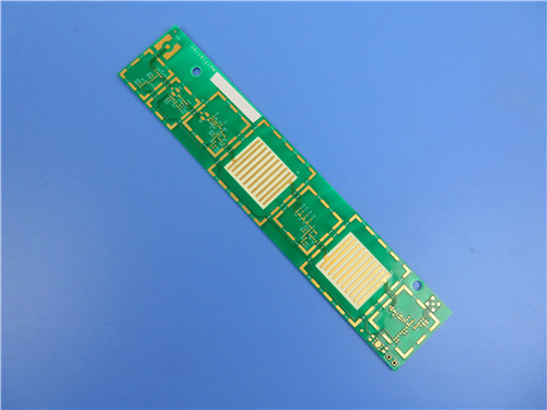
Rogers RO4350B and FR4 Tg180 Hybrid PCB – 1.553mm 8-Layer PCB with Blind and Buried Vias for Automotive Radar and Base Station Antennas
Printed Circuit Boards are custom-made products; the images and specifications provided are for reference only.
1. Product Introduction
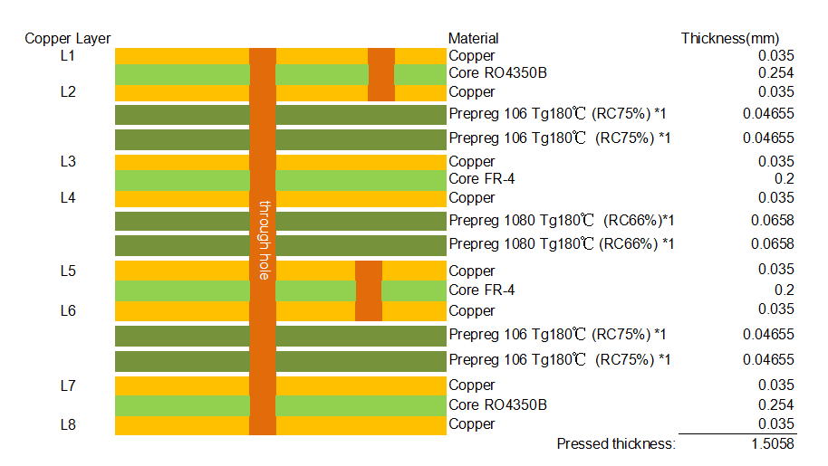
Rogers 8-layer PCB uses a hybrid stackup with 10mil RO4350B laminate on the top and bottom layers, and FR4 (Tg180) in the middle layers. The finished board thickness is 1.553 mm, and the panel size is 120 mm × 30 mm (1 piece per panel). Inner layer copper is 1 OZ, and outer layer finished copper is 1 OZ. Rogers RO4350B and FR4 circuit board features green solder mask, white silkscreen, and ENIG (electroless nickel immersion gold) surface finish. Additional specifications include plated hole copper thickness of 25 µm meeting IPC Class 3 standards, metal edge plating (edge metallization), blind vias from layer 1 to 2, buried vias from layer 5 to 6, and resin plugging for these vias.
2. Product Specification Table
Parameter |
Value / Description |
Layer count |
8 layers |
Material |
Top/bottom: 10mil RO4350B; Middle: FR4 Tg180 |
Finished board thickness |
1.553 mm |
Board dimensions |
120 mm × 30 mm (1 piece) |
Inner layer copper |
1 OZ |
Outer layer finished copper |
1 OZ |
Solder mask |
Green |
Silkscreen |
White |
Surface finish |
ENIG (Electroless Nickel Immersion Gold) |
Plated hole copper thickness |
25 µm |
IPC standard |
Class 3 (IPC-3) |
Special features |
Metal edge plating, blind vias (1-2), buried vias (5-6), resin plug vias |
Metal edge plating provides improved shielding and grounding along the board perimeter. Blind vias connect the outer layer to the first inner layer without penetrating the whole board. Buried vias are completely internal between layers 5 and 6. All blind and buried vias are resin plugged to ensure a planar surface for subsequent lamination and assembly.
3. RO4350B Laminate Introduction
RO4000® series hydrocarbon ceramic laminates are designed for superior high-frequency performance while enabling low-cost circuit fabrication. RO4350B™ is a specific grade within the RO4000 series, specifically designed as a drop-in replacement for RO4003C with RoHS compliant flame-retardant technology for applications requiring UL 94V-0 certification. These materials conform to IPC-4103 slash sheet /10 for RO4003C. RO4350B is a reinforced hydrocarbon/ceramic laminate – not PTFE. It offers low dielectric loss and stable dielectric constant over a broad frequency range, making it ideal for RF microwave circuits, matching networks, and controlled impedance transmission lines. The material has a Tg >280°C (536°F), ensuring stable expansion characteristics over the entire range of circuit processing temperatures. Its thermal coefficient of expansion (CTE) is similar to copper, providing excellent dimensional stability and reliable plated through-hole quality even under severe thermal shock. Unlike PTFE-based materials, RO4350B does not require specialized via preparation processes such as sodium etch. It is a rigid, thermoset laminate that can be processed using standard FR-4 circuit board techniques, including automated handling and scrubbing equipment.
4. Typical Properties of RO4350B
Property |
Value |
Dielectric Constant (Dk) |
(Insert value, typically 3.48 ± 0.05 at 10 GHz) |
Dissipation Factor (Df) |
(Insert value, typically 0.0037 at 10 GHz) |
Thermal Coefficient of Dk |
(Insert value) |
Tg |
>280°C |
CTE (X/Y/Z) |
(Insert values) |
Moisture Absorption |
(Insert value, <0.05%) |
Flame Retardant |
UL 94V-0 |
5. Typical Applications of RO4350B
Cellular base station antennas and power amplifiers, RF identification (RFID) tags, automotive radar and sensors, low-noise block downconverters (LNBs) for direct broadcast satellites, broadband and controlled impedance transmission lines.
6. Fabrication Guidelines for RO4350B (Based on Rogers Recommendations)
Store fully clad RO4350B laminates at room temperature between 50 and 90°F (10 to 32°C). A first-in-first-out inventory system is recommended, and material lot numbers should be tracked through production. For inner layer preparation, RO4350B is compatible with pinned and pinless tooling systems; slotted pins with multiline tooling and post-etch punching meet most registration needs. Surface preparation for photoresist depends on core thickness: thinner cores require chemical cleaning (micro-etch, rinse, dry), while thicker cores work with mechanical scrub systems. The material works with most liquid and dry film photoresists and can be processed through standard develop-etch-strip (DES) systems. For multi-layer bonding, RO4350B cores can be processed through any copper oxide or oxide alternative process and are compatible with most thermosetting and thermoplastic adhesive systems – always follow the adhesive supplier’s bond cycle parameters. Drilling: avoid speeds above 500 SFM. Recommended parameters: surface speed 300–500 SFM (90–150 m/min), chip load 0.002–0.004 inches per revolution, retract rate 500 IPM for tools smaller than 0.0135″ diameter and 1000 IPM for larger tools. Use standard carbide drills. Tool life is typically 2,000–3,000 hits. Standard geometry drills are preferred. Expected hole wall roughness ranges from 8 to 25 µm and remains consistent over thousands of hits. For PTH processing, desmear is typically not required for double-sided boards due to high Tg >280°C; multi-layer boards may require alkaline permanganate or plasma desmear. Etchback of RO4350B layers is not recommended as it may loosen filler particles. Metal deposition does not require special pre-treatment – RO4350B is compatible with electroless copper and direct metallization processes. For high aspect ratio holes, a flash copper plate of 0.00025 inches before imaging may be considered. Copper plating and outer-layer processing: compatible with standard acid copper, tin or tin/lead plating, and any strip/etch/strip (SES) process. Preserve the post-etch surface for good solder mask adhesion. Final metal finishes compatible with RO4350B include ENIG, OSP, and HASL. For routing, use carbide multi-flute spiral chip breaker or diamond cut router bits with surface speeds below 500 SFM and chip load of 0.0010–0.0015 inches per revolution. Copper should be etched away from the routing path to prevent burring. Maximum stack height for routing should be 70% of the actual flute length to allow debris removal. RO4350B laminates can be stored for extended periods at ambient room temperature (55–85°F / 13–30°C), though copper oxidation may occur over time and can be removed with standard micro-etch processes.
7. Understanding Blind Vias and Buried Vias
A blind via is a plated hole that connects an outer layer (layer 1 or 8) to one or more inner layers without going through the entire board thickness. In this design, blind vias are used from layer 1 to layer 2. A buried via is a plated hole that connects two or more inner layers only, with no access from the outer surfaces. Here, buried vias are used from layer 5 to layer 6. Both types are resin plugged to fill the via cavities, preventing solder wicking and ensuring a flat surface for subsequent layer lamination or component placement.
8. Advantages of Blind and Buried Via Design
Using blind and buried vias reduces signal path lengths, improving high-frequency performance and reducing parasitic inductance. They free up routing space on outer layers, allowing higher component density. Resin plugging provides planar surfaces, which is essential for reliable multi-layer bonding and prevents contamination during assembly. Compared to through-hole vias, blind and buried vias enable smaller pad sizes and finer pitch designs.
9. Disadvantages and Considerations
Blind and buried vias increase fabrication complexity and cost because they require sequential lamination and multiple drilling steps. Resin plugging adds additional process control. Designers must carefully plan layer stackups and via structures to ensure manufacturability. Not all PCB suppliers have the capability to produce blind/buried vias with resin plugging, especially on hybrid RO4350B + FR4 stacks.
10. Summary
This Rogers 8-layer RO4350B PCB uses a hybrid stackup of 10mil RO4350B on top and bottom with FR4 Tg180 in the middle. Finished thickness is 1.553 mm, panel size 120 mm × 30 mm. Copper weights are 1 OZ inner and outer. The board has green solder mask, white silkscreen, and ENIG finish. Hole copper is 25 µm, IPC Class 3. Special features include metal edge plating, blind vias (1-2), buried vias (5-6), and resin plug vias. Rogers RO4350B laminate provides low-loss, stable Dk performance with standard FR-4 processing. Key fabrication guidelines: store at room temperature, use standard carbide drills with 300–500 SFM and chip load 0.002–0.004″/rev, avoid etchback, and ensure copper is removed from routing paths to prevent burring.