

 Home
-
Newly shipped PCBs
-
14-Layer Panasonic MEGTRON6 R-5775(N) / R-5670(N) PCB – 2.406mm Impedance Control PCB with Resin Plug and Plated Fill Vias
Home
-
Newly shipped PCBs
-
14-Layer Panasonic MEGTRON6 R-5775(N) / R-5670(N) PCB – 2.406mm Impedance Control PCB with Resin Plug and Plated Fill Vias
14-Layer Panasonic MEGTRON6 R-5775(N) / R-5670(N) PCB – 2.406mm Impedance Control PCB with Resin Plug and Plated Fill Vias
Printed Circuit Boards are custom-made products; the images and specifications provided are for reference only.
1. Product Introduction
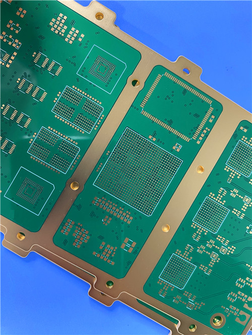
This 14-layer PCB is fabricated with Panasonic MEGTRON6 high-speed, low-loss multilayer material — laminate R-5775(N) and prepreg R-5670(N) using low Dk glass cloth. This high-performance material platform is widely applied in advanced designs such as 12-Layer High-Speed Megtron M6 PCB for 5G, networking, and wireless systems. The finished board thickness is 2.406 mm, and the panel size is 106 mm × 102 mm (1 piece per panel). Inner layer finished copper is 0.5 oz, and outer layer finished copper is 1 oz. The board features green solder mask, white silkscreen, and ENEPIG (Electroless Nickel Electroless Palladium Immersion Gold) surface finish. Additional specifications include compliance with IPC Class 3 standards, five controlled impedance lines, and 0.2 mm vias with resin plug and electroplated fill.
2. Product Specification Table
Parameter |
Value / Description |
Layer count |
14 layers |
Material |
Panasonic MEGTRON6 R-5775(N) laminate / R-5670(N) prepreg |
Finished board thickness |
2.406 mm |
Board dimensions |
106 mm × 102 mm (1 piece) |
Inner layer finished copper |
0.5 OZ |
Outer layer finished copper |
1 OZ |
Solder mask |
Green |
Silkscreen |
White |
Surface finish |
ENEPIG (Electroless Nickel Palladium Immersion Gold) |
IPC standard |
Class 3 |
Impedance control |
5 locations |
Via specification |
0.2 mm diameter, resin plug + electroplated fill |
The five impedance-controlled lines ensure signal integrity for high-speed digital and RF applications. The 0.2 mm vias are first plugged with resin then electroplated flat to provide a smooth surface for subsequent layers and component mounting.
3. Panasonic MEGTRON6 Material Introduction
MEGTRON6 (R-5775(N) laminate and R-5670(N) prepreg) is a high-speed, low-loss multilayer PCB material featuring low Dk glass cloth. It is designed for demanding digital and high-frequency applications requiring excellent signal integrity and minimal insertion loss. The material system provides stable electrical properties over a broad frequency range, low dissipation factor, and high thermal reliability. MEGTRON6 is widely used in high-speed digital backplanes, communication infrastructure, servers, and test equipment.
4. Typical Properties of R-5775(N) Laminate
Property |
Condition |
Typical Value |
Unit |
Test Method |
Thermal |
|
|
|
|
Tg (DSC) |
As received |
185 |
°C |
DSC |
Tg (DMA) |
As received |
210 |
°C |
DMA |
Td (TGA) |
As received |
410 |
°C |
TGA |
T288 (delamination) |
With / without Cu |
>120 |
Min |
IPC TM-650 2.4.24.1 |
CTE α1 (X/Y) |
< Tg |
14–16 |
ppm/°C |
IPC TM-650 2.4.24 |
CTE α1 (Z) |
< Tg |
45 |
ppm/°C |
IPC TM-650 2.4.24 |
CTE α2 (Z) |
> Tg |
260 |
ppm/°C |
IPC TM-650 2.4.24 |
Electrical |
|
|
|
|
Dk @1 GHz |
C-24/23/50 |
3.40 |
– |
IPC TM-650 2.5.5.9 |
Dk @13 GHz |
C-24/23/50 |
3.34 |
– |
IEC 63185 |
Df @1 GHz |
C-24/23/50 |
0.002 |
– |
IPC TM-650 2.5.5.9 |
Df @13 GHz |
C-24/23/50 |
0.0037 |
– |
IEC 63185 |
Volume Resistivity |
C-96/35/90 |
1×10⁹ |
MΩ·cm |
IPC TM-650 2.5.17.1 |
Surface Resistivity |
C-96/35/90 |
1×10⁸ |
MΩ |
IPC TM-650 2.5.17.1 |
Physical |
|
|
|
|
Water Absorption |
D-24/23 |
0.14 |
% |
IPC TM-650 2.6.2.1 |
Peel Strength (1oz H-VLP) |
As received |
0.8 |
kN/m |
IPC TM-650 2.4.8 |
Flammability |
C-48/23/50 |
94V-0 |
– |
UL |
5.R-5670(N) Prepreg Summary
R-5670(N) prepreg is available with glass cloth styles 1035, 1078, 2013, and 2116. Resin content ranges from 56% to 77%, and thickness from 60 to 132 μm. Dielectric constant (Dk) across 1–58 GHz is between 3.08 and 3.40, and dissipation factor (Df) between 0.002 and 0.0046. These properties make R-5670(N) an excellent bonding material for multi-layer constructions requiring consistent low-loss performance.
6. Understanding Impedance Control – Types, Importance and Implementation
Impedance control refers to the management of characteristic impedance along a transmission line to match source and load impedances, thereby minimizing signal reflections, distortion, and power loss. In high-speed digital and RF circuits, maintaining consistent impedance is critical for signal integrity.
6.1 Common types of impedance:
Single‑ended (or characteristic) impedance (Z₀): The impedance of a signal trace referenced to ground. Typical values are 50Ω (most common for RF, wireless, and high‑speed digital) and 75Ω (video, cable TV). In this 14‑layer MEGTRON6 PCB, some of the five impedance‑controlled lines are likely single‑ended.
Differential impedance (Zdiff): The impedance measured between two complementary signal traces (e.g., D+, D‑) that carry opposite polarities. Common values are 90Ω (USB 2.0/3.x, PCIe) and 100Ω (Ethernet, LVDS, DDR). The differential pair provides better noise immunity.
Common mode impedance (Zcm): The impedance of the two traces in a differential pair when driven with the same signal phase. It is less frequently specified but important for common‑mode noise filtering.
Coplanar waveguide (CPW) impedance: Used for RF traces where ground is placed on the same layer alongside the signal line. Values typically 50Ω.
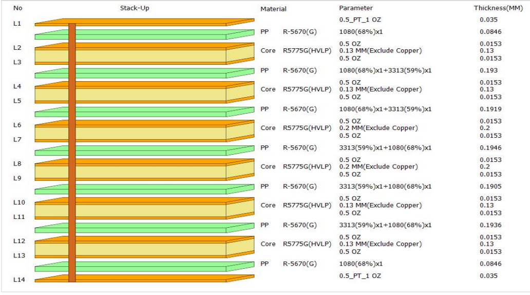
Impedance Control Stackup & Simulation Results for This 14-Layer MEGTRON6 PCB
Below are the detailed impedance simulation models and final control parameters for the 5 differential 100Ω lines specified in the design, split by transmission line type:
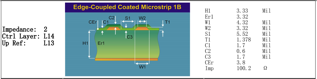
1. Edge-Coupled Coated Microstrip (Top/Bottom Outer Layers)
These two models correspond to the outermost signal layers (L1, L14) of the stackup, using a coated microstrip structure with solder mask over the traces.
Figure 1: Edge-Coupled Coated Microstrip 1B (Impedance 1, Ctrl Layer L1, Down Ref L2) – 100.2Ω differential impedance
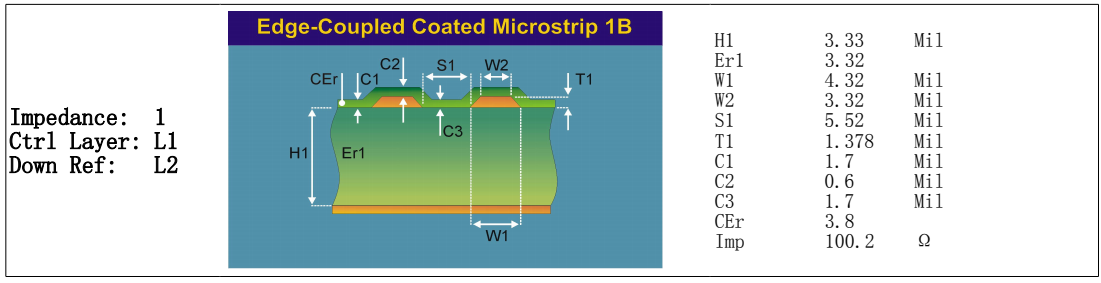
Figure 2: Edge-Coupled Coated Microstrip 1B (Impedance 2, Ctrl Layer L14, Up Ref L13) – 100.2Ω differential impedance
2. Edge-Coupled Offset Stripline (Inner Signal Layers)
These three models correspond to the inner signal layers (L5, L10, L12) of the stackup, using an offset stripline structure sandwiched between two reference planes.
Figure 3: Edge-Coupled Offset Stripline 1B1A (Impedance 3, Ctrl Layer L5, Up Ref L4, Down Ref L6) – 100.8Ω differential impedance
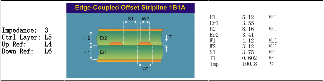
Figure 4: Edge-Coupled Offset Stripline 1B1A (Impedance 4, Ctrl Layer L10, Up Ref L9, Down Ref L11) – 100.74Ω differential impedance
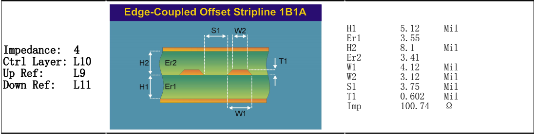
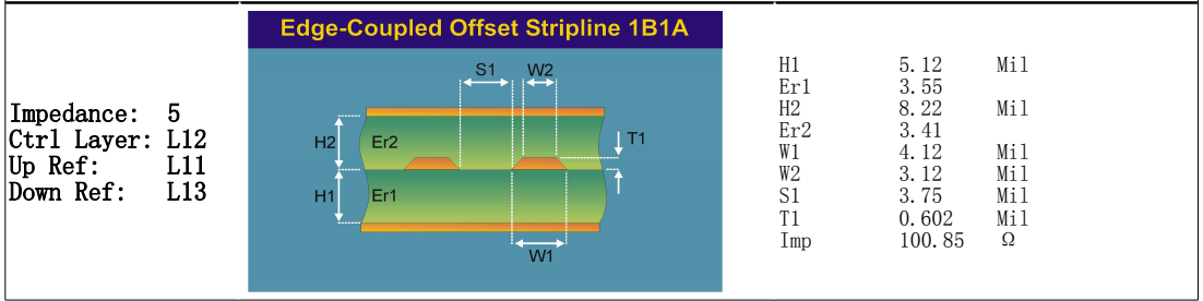
Figure 5: Edge-Coupled Offset Stripline 1B1A (Impedance 5, Ctrl Layer L12, Up Ref L11, Down Ref L13) – 100.85Ω differential impedance
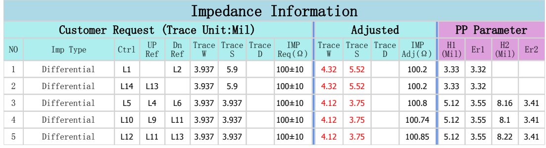
3. Final Impedance Control Summary Table
This table consolidates the customer requirements, adjusted trace geometry, and dielectric stackup parameters for all 5 impedance-controlled lines, confirming compliance with the 100Ω ±10% tolerance.
Figure 6: Impedance Information Summary – Customer Request vs. Adjusted Values & PP Parameters
6.2 How impedance is controlled in PCB fabrication:
Impedance depends on trace width (W), dielectric thickness (H), dielectric constant (Dk) of the material, trace thickness (T), and the spacing between differential traces (S). For MEGTRON6 with Dk ~3.4, the designer calculates target impedances, and the fabricator adjusts trace geometry and layer stackup accordingly. Process control (etching accuracy, lamination pressure, resin content) is essential to achieve ±10% tolerance.
In this 14-layer Panasonic MEGTRON6 PCB, five locations are designated for impedance control. These are all 100Ω differential lines (as confirmed by the simulation results above), designed for high-speed interfaces like Ethernet, LVDS, or DDR. Proper impedance design ensures minimal signal reflections, lower bit error rates, and reliable operation at high data rates.
7. Material Storage and Handling Guidelines for MEGTRON6
Laminate R-5775(N) should be stored flat in a cool, dry environment. Avoid bending or scratching the laminate surface. When possible, keep the laminate in its original container. Prepreg R-5670(N) must be stored flat in a cool, dry, controlled environment at 73°F (23°C) or less and 50% RH or less. For extended storage, prepreg should be kept at a reduced temperature of 41°F (5°C). Opened bags of prepreg must be resealed immediately. Prepreg should not be exposed to open environments for more than 8 hours total cumulatively under the above conditions, unless otherwise agreed between user and supplier.
8. Surface Preparation and Inner Layer Bond Treatment
For laminate surface preparation, regular shiny copper can be cleaned using industry standard chemical or mechanical cleaning processes. Reverse treat copper should be cleaned using industry standard chemical clean only. For inner layer bond treatment, black or brown oxide can be used. If black oxide is applied, verify that peel strength is acceptable for the intended usage. An alternative oxide treatment using organic coating with a peroxide/sulfuric etch technology is preferred because it provides more consistent bonding and reduces the risk of pink ring.
9. Drying Process for Inner Layers
After processing, inner layers must be completely dried to remove any absorbed moisture or surface moisture. A racked bake at 225°F (105°C) for 20 to 30 minutes is preferred. For conveyorized alternative oxide processing, some equipment may have sufficient in-line drying capability, but a separate racked bake is still recommended to ensure full moisture removal before lamination.
10.Resin Plug and Electroplated Fill Vias for 0.2mm Holes
This 14-layer MEGTRON6 PCB uses 0.2 mm diameter vias that are first filled with a conductive or non-conductive resin (resin plug) and then electroplated over to create a flat, coplanar surface. Resin plug prevents solder wicking, trapped air, or contamination inside the via. The subsequent electroplating fills any remaining depression, resulting in a solid copper surface. This process is critical for high-density designs where vias are placed in solder pads (via-in-pad) or under BGAs.
11.Summary
This 14-layer PCB is built on Panasonic MEGTRON6 high-speed low-loss material (laminate R-5775(N), prepreg R-5670(N)) with a finished thickness of 2.406 mm and panel size 106 mm × 102 mm. Copper weights are 0.5 OZ inner and 1 OZ outer. The board has green solder mask, white silkscreen, and ENEPIG finish. It meets IPC Class 3, includes five impedance-controlled lines, and features 0.2 mm vias with resin plug and electroplated fill. MEGTRON6 provides Dk 3.34–3.40, Df 0.002–0.0037, Tg 185°C (DSC), Td 410°C, and UL 94V-0 flammability. Key processing notes: store laminate flat in cool/dry conditions, keep prepreg at ≤73°F/50% RH with limited open-air exposure (≤8 hours), use chemical cleaning for reverse treat copper, prefer peroxide/sulfuric alternative oxide, and bake inner layers at 225°F for 20-30 minutes.