


 Home
-
Newly shipped PCBs
-
2-Layer F4BTM298 High Frequency PCB 10mil Ceramic Filled PTFE Board with ENIG for Phased Array Antennas and Satellite Communication
Home
-
Newly shipped PCBs
-
2-Layer F4BTM298 High Frequency PCB 10mil Ceramic Filled PTFE Board with ENIG for Phased Array Antennas and Satellite Communication
2-Layer F4BTM298 High Frequency PCB 10mil Ceramic Filled PTFE Board with ENIG for Phased Array Antennas and Satellite Communication
Printed Circuit Boards are custom-made products; the images and specifications provided are for reference only.
1. Introduction
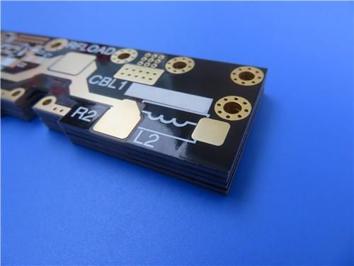
Wangling F4BTM298 PCB is a 2-Layer rigid high-frequency printed circuit board built on 10mil F4BTM298 fiberglass & nano-ceramic loaded PTFE core, specially designed for microwave, radar and satellite communication hardware. 0.3mm finished-thickness F4BTM298 circuit board comes with Immersion Gold surface finish, fully complies with IPC-Class-2 manufacturing standards and supports global mass production and delivery. Developed upgraded from standard F4BM substrate, Wangling F4BTM298 integrates uniformly dispersed low-loss nano-ceramic fillers into PTFE resin and woven glass cloth, balancing stable low dissipation factor, upgraded heat resistance, low CTE and reliable insulation performance. Equipped with standard ED copper foil, F4BTM298 2-Layer PCB fits RF projects without strict PIM demands, widely adopted for phased array antennas, phase shifters, power dividers, base station antennas and satellite communication feed networks. Stable Dk 2.98 performance and tight dimensional tolerance make the F4BTM298 circuit board ideal for mass-fabricated millimeter-wave RF modules.
2. Core Electrical & Thermal Features
- Controlled Dielectric Constant (Dk): 2.98±0.06 at 10GHz
- Low Dissipation Factor (Df): 0.0018 measured at 10GHz
- Three-axis CTE specification: X-axis 15 ppm/°C, Y-axis 16 ppm/°C, Z-axis 78 ppm/°C (-55°C ~ 288°C)
- Ultra-low TCDK: -78 ppm/°C within -55°C to 150°C operating range
- Moisture Absorption Rate: ≤0.05%
- UL 94-V0 flame retardant rating
- Fiberglass & nano-ceramic composite structure for balanced thermal and electrical stability
- Radiation-resistant and low vacuum outgassing material property
- Batch-consistent dielectric performance for repeatable RF signal integrity
- Standard ED copper foil matching for general non-PIM RF circuit layouts
3. Key Product Advantages
- Optimized nano-ceramic filling raises Dk value while retaining ultra-low dielectric loss for compact RF circuit design on F4BTM298 PCB
- Lower thermal expansion coefficient minimizes dimensional shift and soldering defects during mass production of 2-Layer F4BTM298 boards
- Improved heat resistance and insulation strength extend service life of radar and satellite communication modules built on F4BTM298 substrate
- Ultra-low moisture absorption avoids electrical parameter drift under variable humidity environments for F4BTM298 PCB assemblies
- UL 94-V0 flame retardant characteristic meets safety requirements for aerospace and base station RF equipment
- F4BTM298 adopts cost-effective ED copper foil, perfect for high-volume projects without strict PIM specifications
- Compatible with standard PTFE PCB fabrication processes, supporting fine trace and dense hole processing on all F4BTM298 2-Layer boards
- Mandatory 100% electrical testing before shipment guarantees full connectivity for every F4BTM298 PCB order
4.PCB Construction Details
Item |
Specification |
Base Material |
Wangling F4BTM298, 10mil (0.254 mm) ceramic filled PTFE copper clad laminate |
Layer Configuration |
2-Layer Rigid PCB |
Board Outline Size |
109mm × 54.5mm, ±0.15mm tolerance, single piece standard F4BTM298 PCB dimension |
Minimum Trace / Space |
6 mils / 9 mils |
Minimum Hole Size |
0.4mm |
Via Type |
Through vias only, blind vias not included |
Finished Board Thickness |
0.3mm |
Outer Copper Weight |
1oz (1.4 mils) ED copper foil |
Via Plating Thickness |
20 μm copper plating |
Surface Finish |
Immersion Gold, standard surface treatment for F4BTM298 PCB |
Top Silkscreen |
White ink printing |
Bottom Silkscreen |
None |
Top Solder Mask |
Black solder mask coating |
Bottom Solder Mask |
No solder mask applied |
Pre-Delivery Inspection |
100% full electrical continuity test for all F4BTM298 circuit boards |
5. PCB Stackup
2-Layer rigid F4BTM298 PCB layer sequence from top to bottom surface:
- Copper Layer 1: 35 μm ED copper foil
- F4BTM298 Dielectric Core: 0.254 mm (10mil)
- Copper Layer 2: 35 μm ED copper foil This 10mil thin core forms the complete 0.3mm finished thickness F4BTM298 RF PCB.
6. PCB Layout Statistics
- Total Mounted Components: 26
- Total Pads: 87
- Through Hole Pads: 49
- Top SMT Pads: 38
- Bottom SMT Pads: 0
- Conductive Through Vias: 31
- Independent Electrical Nets: 2 The rich pad and via layout fits multi-component RF modules on compact 0.3mm F4BTM298 2-Layer PCB.
7. Fabrication Artwork & Quality Standard
- Required Production File Format: Gerber RS-274-X
- Enforced Quality Compliance: IPC-Class-2, implemented for all F4BTM298 PCB batches
- Global Supply Support: Worldwide prototype & mass production for Wangling F4BTM298 PCB
8. Typical Application Scenarios
- Microwave, RF and airborne radar systems manufactured on F4BTM298 2-Layer PCB
- RF phase shifter circuit boards built with F4BTM298 ceramic filled laminate
- Power dividers, couplers and RF combiners using F4BTM298 substrate
- Antenna feed network hardware based on 0.3mm F4BTM298 Immersion Gold PCB
- Phase-sensitive antennas and phased array antenna RF boards
- Satellite communication transceiver modules with F4BTM298 dielectric core
- Cellular base station antenna circuit assemblies
9. Copper Clad Laminate Knowledge: F4BTM298
9.1 F4BTM Series Material Overview
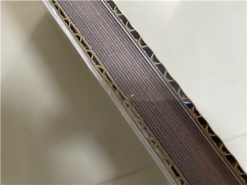
Wangling F4BTM298 belongs to the fiberglass fabric & nano-ceramic filled PTFE copper clad laminate lineup, alongside its variant F4BTME298. F4BTM298 substrate is manufactured by mixing woven glass fiber, special nano-ceramic fillers and PTFE resin, then processed via precise high-pressure lamination. Upgraded from classic F4BM base material, F4BTM298 adds high-Dk low-loss nano-ceramics to lift dielectric constant, thermal resistance and thermal conductivity, while retaining inherent low dissipation factor of PTFE dielectric.
F4BTM298 and F4BTME298 share identical 10mil dielectric core, the only difference lies in copper foil matching: F4BTM298 is equipped with standard ED electrodeposited copper foil, targeting general RF projects without strict Passive Intermodulation (PIM) requirements. By contrast, F4BTME298 uses RTF reverse-treated copper foil to deliver superior PIM performance, finer trace control and lower conductor loss for high-precision antenna hardware.
The full F4BTM series supports customizable Dk ranging from 2.98 to 3.5, with abundant thickness options and flexible dimensions to cut overall project cost. All variants feature radiation resistance and low outgassing, suitable for aerospace and long-term outdoor RF equipment. Mass-volume mature production makes F4BTM298 a cost-effective alternative to imported high-frequency laminates.
9.2 Core CCL Performance Features
- Tunable Dk range from 2.98 to 3.5 to match diverse RF circuit design demands
- Nano-ceramic reinforced formula enhances overall thermal and electrical performance of F4BTM298
- F4BTME variant delivers outstanding PIM performance for high-end antenna projects
- Multiple standardized dielectric thickness selections for flexible stackup design
- Customizable board dimensions to optimize manufacturing cost of F4BTM298 PCB
- Mature mass production process ensures stable pricing and short lead time
- Radiation resistant & low vacuum outgassing for space and airborne radar applications
9.3 Application Range for F4BTM298 Laminate
- Microwave, RF and multi-type radar system circuit boards
- RF phase shifter modules fabricated on F4BTM298 substrate
- Power dividers, couplers and RF signal combiners
- Antenna feed network PCBs for satellite and base station hardware
- Phase-sensitive antennas and phased array antenna assemblies
- Satellite communication positioning and signal transmission equipment
- Cellular base station antenna RF circuit boards
10.F4BTM/F4BTME Series Full Specification Table
Item |
Specification Details |
Optional Copper Foil & Thickness |
1. F4BTM (ED Copper Foil): 0.5OZ (0.018mm), 1OZ (0.035mm), 1.5OZ (0.05mm), 2OZ (0.07mm)2. F4BTME (Reverse RTF Copper Foil): 0.5OZ (0.018mm), 1OZ (0.035mm) |
Available Panel Dimensions |
Conventional sizes: 460×610mm, 600×500mm, 914×1220mmNote: 914×1220mm size is unavailable for substrate thickness ≥ 4.0mm |
Standard Thickness & Tolerance (0.254~1.524mm) |
0.254mm (Min): ±0.02mm|0.508mm: ±0.04mm|0.762mm/0.8mm/1.0mm/1.016mm: ±0.05mm|1.27mm/1.524mm: ±0.06mm |
Standard Thickness & Tolerance (2.0~12.0mm) |
2.0mm: ±0.075mm|3.0mm: ±0.09mm|4.0mm/5.0mm: ±0.1mm|6.0mm: ±0.12mm|8.0mm: ±0.15mm|10.0mm: ±0.18mm|12.0mm: ±0.2mm |
Thickness Instruction |
All standard thicknesses can be produced as total copper-clad thickness or dielectric core thickness. Please specify the thickness type when placing orders. Non-standard thicknesses are customizable upon request. |
Metal Base Model |
F4BTM(E)-2-A***-CU (Copper Base), F4BTM(E)-2-A***-AL (Aluminum Base) |
Base Metal Parameter |
1. Copper Base (Red Brass/Brass): Specific Gravity: 8.9, Thermal Conductivity: 3802. Aluminum Base: Specific Gravity: 2.7, Thermal Conductivity: 180 |
Metal Base Available Thickness |
0.48mm, 0.98mm, 1.48mm, 1.98mm, 2.98mm, 3.98mm (Custom thickness available) |
Metal Base Thickness Tolerance |
+0.02mm / -0.05mm |
Metal Base Available Dimensions |
460×610mm, 460×305mm (Custom sizes available) |
Product Feature |
One side of the dielectric layer is covered with copper foil, and the other side is bonded with aluminum/copper base for shielding and heat dissipation. |
Model Example |
1. F4BTM298-AL: F4BTM298 substrate with aluminum base2. F4BTME298-CU: F4BTME298 substrate with copper base |
11.Summary
F4BTM298 2-Layer High Frequency PCB delivers balanced low-loss electrical performance and reliable thermal stability for microwave, radar and satellite communication RF devices. Constructed on 10mil Wangling F4BTM298 nano-ceramic glass fiber PTFE core with Dk 2.98 and low Df 0.0018, this 0.3mm thin circuit board adopts Immersion Gold surface finish and meets IPC-Class-2 standards for worldwide delivery. Featuring low CTE, UL 94-V0 flame retardant grade and cost-effective ED copper foil configuration, F4BTM298 RF circuit board is an ideal base board for phased array antennas, phase shifters, power dividers, base station antennas and satellite communication feed network projects without strict PIM standards.
Tags:Wangling F4BTM298 PCB, 2-Layer 0.3mm F4BTM298 RF PCB, 10mil Dk 2.98 F4BTM298 Laminate, F4BTM298 Immersion Gold Circuit Board, IPC-Class-2 F4BTM298 High Frequency PCB, Ceramic Filled PTFE F4BTM298 Substrate, Phased Array Antenna F4BTM298 PCB, Satellite Communication F4BTM298 RF Board