


 Home
Home
What is Solder Mask Opening/Clearance in PCB?
 December 16,2025
To understand solder mask opening, we first need to grasp the concept of the solder mask itself. Commonly known as the green layer on a PCB, the solder mask is a protective lacquer applied to the copper traces to prevent oxidation, short circuits, and solder bridges during assembly. It is applied as a negative layer, meaning the openings or "clearances" in this layer are where the copper is intentionally exposed for soldering components. These exposed areas are precisely the "solder mask openings."
1.The Role of Solder Mask in Manufacturing
The solder mask plays a crucial role in minimizing soldering defects, especially during reflow soldering. A key design requirement is managing the clearance or air gap between the mask and the copper pads. While it may be preferable to have a single, large mask opening around groups of pads for some components, this isn't always feasible with high-density designs.
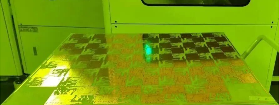
PCB panel with solder mask opening
2.Design Considerations for Dense Components
The spacing between pins on fine-pitch components, like Quad Flat Packs (QFPs) or Ball Grid Arrays (BGAs), demands special attention. For BGAs, a specific technique called Solder Mask Defined (SMD) pads is often used. Here, the solder mask covers the spaces between the pads, touching and slightly overlapping the edges of the copper pads. This helps contain the solder ball and prevent bridging. In contrast, a Non-Solder Mask Defined (NSMD) pad leaves a clearance around the copper, which can be better for adhesion but requires precise process control.
SMD vs NSMD Pad Design Comparison
Feature |
Solder Mask Defined (SMD) |
Non-Solder Mask Defined (NSMD) |
Recommended Application |
Pad Structure |
Mask opening is smaller than or equal to the copper pad. |
Mask opening is larger than the copper pad. |
Critical for BGA and fine-pitch QFP designs. |
Solder Mask Overlap |
Mask overlaps the copper pad edge by 0.025-0.050mm. |
Clearance of 0.075-0.100mm between mask and copper pad. |
High-density interconnects (HDI). |
Copper Pad Size |
Typically larger to accommodate mask overlap. |
Typically smaller, as copper defines the final pad. |
Flip-chip and Chip-Scale Package (CSP). |
Solder Joint Reliability |
Better resistance to pad cratering under thermal stress. |
Stronger mechanical shear strength due to full copper exposure. |
Automotive (thermal cycling) vs. consumer (mechanical stress). |
Manufacturing Complexity |
Higher; requires critical mask-to-pad registration accuracy. |
Lower; more forgiving of minor registration errors. |
Standard consumer electronics. |
Risk of Solder Bridging |
Lower; the mask physically contains the solder ball. |
Higher; relies on precise solder paste volume control. |
Pitches of 0.4mm |
Most modern surface-mount PCBs use a liquid photoimageable solder mask (LPI). It's essential that the mask has a low profile. If it's thicker than approximately 0.04mm, it can interfere with the accurate application of solder paste, particularly for components with very fine pitch.
3.The Opening Itself: A Matter of Precision
The term "solder mask opening" refers to the size of the exposed copper area meant for soldering. A related term is "solder mask web" or "dam," which is the width of the mask material left between two openings. If this dam is too small, it can lead to mask slippage during manufacturing, exposing areas not meant for solder and potentially causing shorts.
Standard practice is to design the mask opening to be 0.15mm larger than the copper pad on all sides. This creates a consistent 0.07mm gap between the pad edge and the mask, ensuring full pad exposure while maintaining a reliable mask dam.
4.Why Are These Openings Necessary?
The reasons for creating these openings are fundamental to PCB functionality:
For Soldering: This is the primary reason. The openings provide clean, exposed copper for solder paste application and component terminal attachment, forming reliable electrical and mechanical connections.
For Plated Through-Holes (PTHs): Openings are required on via holes and component holes if they are intended to be filled with solder during assembly ("tented" vias are an exception). For finishes like ENIG (Electroless Nickel Immersion Gold), the opening is necessary for the plating process to reach the copper inside the hole.
For Surface Finish Application: Openings allow for the application of final surface finishes like HASL, ENIG, or Immersion Tin directly onto the copper pads, protecting them before soldering.
5.Conclusion
In summary, solder mask openings are a critical, precision-designed aspect of PCB fabrication. They balance the need to protect the board with the requirement to expose specific areas for reliable soldering and surface treatment, directly impacting the quality, reliability, and manufacturability of the final electronic product.
Founded in 2003, Shenzhen Bicheng Electronics Technology Co., Ltd is an established high frequency PCB supplier and exporter in Shenzhen, China, serving customers worldwide.
We are devoted to delivering high-frequency PCB products and solutions of the highest quality, along with customized service. Get in touch with us to start your project !
Visit https://www.bicheng-enterprise.com to learn more.
Contact Vicky at v.xie@BTL_VickyXie.com to unlock its full potential.