


 Home
Home
What Factors Should Be Considered in Stack-up Design for Multi-layer PCBs?
 December 10,2025
1.Electrical Performance
Impedance Control
Different circuit signals may require specific impedance values to ensure signal integrity. For example, differential signals in high-speed digital circuits typically need to be controlled at around 100Ω differential impedance. Properly arrange the distance between signal layers and reference planes (power or ground layers), dielectric thickness, and trace width to meet the required impedance specifications. Professional impedance calculation software can be used to precisely design the stack-up structure based on parameters such as the dielectric constant of the PCB material.
Signal Integrity
Crosstalk between adjacent signal layers can affect signal quality. Separate high-speed signal layers from low-speed signal layers, and insert ground or power layers between high-speed signal layers to provide shielding and reduce crosstalk. For instance, in a 6-layer PCB, high-speed digital signal layers can be placed in the middle, surrounded by ground layers above and below, to minimize electromagnetic radiation and susceptibility to external interference.
Power and Ground Plane Distribution
Properly plan the layout of power and ground planes to provide stable power supply and reliable grounding for the circuit. Power planes should evenly distribute power to various circuit modules, while ground planes should provide low-impedance return paths. For multi-layer PCBs with multiple power domains, different power planes need to be partitioned and arranged to avoid interference between them. Additionally, ensure the integrity of power and ground planes to reduce noise.
2.Thermal Management
Heat Conduction
For components with high power consumption or areas generating significant heat, thermal management must be considered. Place ground and power layers close to heat-generating components to leverage the good thermal conductivity of metal layers for heat dissipation. For example, when a PCB includes high-power chips, large-area copper foils can be placed in the underlying layers as heat dissipation layers, transferring heat through vias to other layers and dissipating it into the air.
Thermal Via Design
Properly designed thermal vias in the PCB can enhance heat dissipation. Thermal vias can be through-holes, transferring heat from one side of the PCB to the other to increase the heat dissipation area. The layout and number of thermal vias should be determined based on the location and heat generation of components, without compromising the mechanical strength or electrical performance of the PCB.
3.Manufacturing Process
Lamination Process Compatibility
Stack-up design must consider the requirements of the lamination process during PCB manufacturing. Different materials may require varying lamination parameters (e.g., temperature, pressure, time). Ensure that all layers bond properly during lamination without issues like delamination or blistering. For example, when laminating special high-frequency materials with standard FR-4 materials, process parameters may need adjustment to accommodate different material properties.
Processing Precision
The stack-up structure can affect the processing precision during PCB manufacturing. For example, the accuracy of via fabrication is related to the PCB thickness. Thicker PCBs may require stricter drilling precision control to ensure via quality and reliable electrical connections. Trace width and spacing precision can also be influenced by the stack-up structure. During design, consider the minimum trace width and spacing achievable by the manufacturing process.
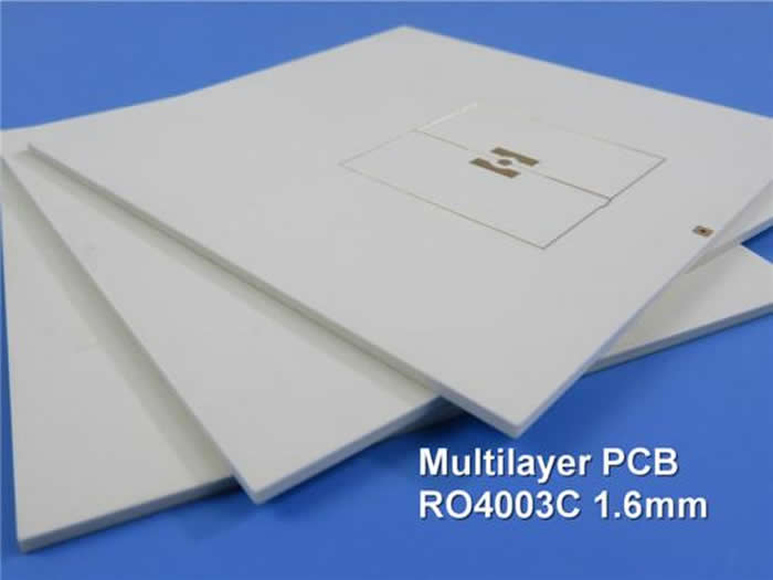
4-Layer RO4003C and FR4 PCB
4.Cost Considerations
Material Selection
Different PCB materials vary significantly in price. Choose the appropriate material based on product performance requirements and budget constraints. For instance, high-performance high-frequency materials are more expensive. If the product does not require high-frequency performance, cost-effective standard FR-4 materials can be used. Also, consider the material thickness. Thicker materials are generally more expensive but may be necessary for applications requiring better mechanical strength or thermal performance.
Layer Count Determination
Increasing the number of PCB layers provides more routing space and better performance but also raises costs. Determine the appropriate layer count by considering circuit complexity and signal requirements. For simple circuits, a 4-layer PCB may suffice, while complex high-speed digital systems may require 6 or more layers. Minimize unnecessary layers to reduce costs without compromising performance.
Reference Table: Common Stack-up Structures for Impedance Control
Layer Count |
Recommended Stack-up Structure (Top to Bottom) |
Typical Impedance Control Capability |
Application Scenarios |
Cost Tier |
4-Layer |
Sig1 / GND / PWR / Sig2 |
Single-ended 50Ω, Differential 100Ω |
Mid-to-low speed digital circuits, General consumer electronics |
Economy |
6-Layer |
Sig1 / GND / Sig2 / PWR / GND / Sig3 |
Precision Control (±10%) |
High-speed digital interfaces (USB 3.0, HDMI) |
Standard |
8-Layer |
Sig1 / GND / Sig2 / GND / PWR / Sig3 / GND / Sig4 |
High Precision (±7%) |
RF front-end, High-speed SerDes (PCIe) |
High-Performance |
10+ Layers |
Multiple GND/PWR layers alternating |
Ultra Precision (±5%) |
Server motherboards, Communication base stations |
|
5. Electromagnetic Compatibility (EMC)
Shielding Layer Configuration
Properly configure shielding layers in the stack-up. For example, ground layers can act as shielding layers, reducing the impact of external electromagnetic interference on internal circuits and preventing electromagnetic radiation from internal circuits from affecting the external environment. For products with high EMC requirements, such as medical or communication devices, additional shielding layer designs may be necessary, such as adding metal shields on the outer layers or using materials with shielding properties.
Ground and Power Plane Layout
The layout of ground and power planes should enhance EMC performance. For example, dividing ground planes into multiple regions and connecting them with low-impedance paths can improve shielding effectiveness, reducing electromagnetic radiation and crosstalk. Power planes should avoid forming large loop areas to minimize electromagnetic radiation.
Founded in 2003, Shenzhen Bicheng Electronics Technology Co., Ltd is an established high frequency PCB supplier and exporter in Shenzhen, China, serving customers worldwide.
We are devoted to delivering high-frequency PCB products and solutions of the highest quality, along with customized service. Get in touch with us to start your project !
Visit https://www.bicheng-enterprise.com to learn more.
Contact Vicky at v.xie@BTL_VickyXie.com to unlock its full potential.