


 Home
Home
Why Via Filling Matters in Modern PCB Manufacturing?
 December 5,2025
Conductive vias serve as critical interconnects between PCB layers, enabling complex circuit routing. With electronics evolving toward higher density and miniaturization, via filling has transitioned from an optional process to an essential manufacturing requirement. This article explains why via filling is crucial and how different implementation methods affect PCB performance.
1.Core Reasons for Via Filling Implementation
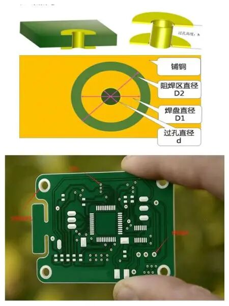
PCB Via Structure Diagram
Short Circuit Prevention: During wave soldering, unfilled vias allow molten solder to flow through to the opposite board side, creating potential short circuits. This risk is particularly acute for BGAs and fine-pitch components.
Solder Paste Containment: In surface mount technology (SMT) assembly, unfilled vias allow solder paste migration during reflow, leading to poor solder joints and reduced reliability.
Testing Compatibility: Automated testing systems often use vacuum suction for board positioning. Properly filled vias create the sealed surface required for reliable electrical testing.
Signal Integrity Enhancement: In high-frequency applications, filled vias minimize impedance discontinuities and reduce signal reflections at via transitions.
2.Technical Requirements for Quality Via Filling
Plating Specifications: For solderable vias, tin-lead plating must achieve minimum 4µm thickness without solder mask contamination
Surface Standards: Filled vias must present completely flat surfaces (±1 mil tolerance) without solder beads, rings, or voids
Material Compatibility: Filling materials must withstand thermal cycling and chemical exposure during subsequent processing
3. Implementation Methods: Technical Comparison
Traditional Pre-HAL Filling Process
This established method involves specialized aluminum stencil fabrication for precise via filling before solder leveling. While ensuring excellent surface flatness, this approach requires additional plating thickness and specialized grinding equipment, increasing manufacturing complexity.
Modern Simultaneous Filling Approach
Contemporary manufacturing often employs modified solder mask printing to achieve via filling and surface coating in a single operation. This streamlined process reduces handling while maintaining quality through:
Optimized ink viscosity control
Precision stencil design
Controlled curing parameters
This integrated approach significantly improves manufacturing efficiency while meeting the flatness requirements for advanced component packaging.
4. Selection Guidelines for Different Applications
Application Context |
Recommended Method |
Key Benefits |
High-density BGAs |
Pre-HAL epoxy filling |
Superior surface planarity |
Cost-sensitive designs |
Simultaneous solder mask filling |
Reduced processing steps |
Thermal management vias |
Conductive paste filling |
Enhanced heat dissipation |
High-frequency circuits |
Controlled dielectric filling |
Improved signal integrity |
5. Future Trends and Considerations
As PCB technology advances toward ultra-high density interconnects (UHDI) and embedded component designs, via filling methodologies continue evolving. Emerging approaches include laser-assisted filling and nano-material composites, offering enhanced precision and performance characteristics.
6. Conclusion
Via filling represents a critical manufacturing step that directly impacts PCB reliability, manufacturability, and performance. Understanding the technical considerations behind different filling methods enables optimal selection for specific application requirements, ensuring robust PCB performance in increasingly demanding electronic environments.
Founded in 2003, Shenzhen Bicheng Electronics Technology Co., Ltd is an established high frequency PCB supplier and exporter in Shenzhen, China, serving customers worldwide.
We are devoted to delivering high-frequency PCB products and solutions of the highest quality, along with customized service. Get in touch with us to start your project !
Visit https://www.bicheng-enterprise.com to learn more.
Contact Vicky at v.xie@BTL_VickyXie.com to unlock its full potential.