


 Home
Home
PCB Copper Pour Guide: Solid vs Grid - Which Should You Choose?
 November 28,2025
PCB copper pour refers to filling unused spaces on a circuit board with solid copper, using these areas as a reference plane. This process is also known as "copper filling."
The key benefits of copper pour are clear: it reduces ground impedance to enhance anti-interference performance, lowers voltage drop for improved power efficiency, and minimizes loop area when connected to the ground. Additionally, most PCB manufacturers require designers to add copper pour (either solid or grid) to empty board areas to prevent warping during soldering.
However, improper copper pour can do more harm than good. For high-frequency circuits, the distributed capacitance of PCB traces becomes significant. When a trace’s length exceeds 1/20 of the noise frequency’s wavelength, it creates an "antenna effect," allowing noise to radiate outward. Poorly grounded copper pour will act as a noise transmitter. In high-frequency designs, never assume a single ground connection is sufficient—use vias spaced less than λ/20 to ensure reliable grounding with the multi-layer board’s ground plane. When done correctly, copper pour serves dual purposes: increasing current capacity and shielding against interference.
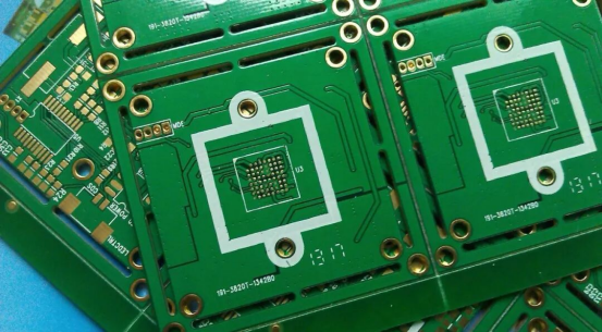
Figure 1: PCB with Copper Pour
2. Two Types of Copper Pour
Copper pour primarily comes in two forms: solid copper pour and grid copper pour. There’s no one-size-fits-all answer to which is better—your choice depends on your design needs.
Solid copper pour offers both high current capacity and strong shielding. However, large solid copper areas may cause the board to warp or bubble during wave soldering. To mitigate this, manufacturers typically add slots to relieve stress in solid copper regions.
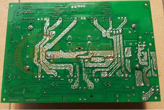
Figure 2: Solid Copper Pour
Grid copper pour (made of crisscrossing traces) prioritizes shielding over current capacity. Its open structure improves heat dissipation by reducing copper surface area while still providing electromagnetic shielding—making it ideal for touch-sensitive circuits.
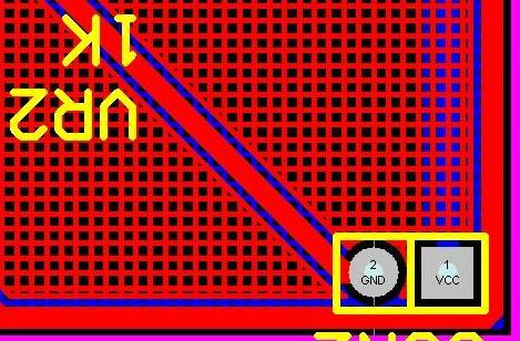
Figure 3: Grid Copper Pour
A critical note: Grid traces have an "electrical length" (calculated by dividing physical length by the signal’s frequency). At low frequencies, this has little impact. But if the grid’s electrical length matches the operating frequency, it can disrupt circuit performance by radiating interfering signals.
3. Summary: Solid vs Grid Copper Pour
Copper Pour Type |
Core Functions |
Ideal Applications |
Key Considerations |
Solid Copper Pour |
High current capacity + strong interference protection |
Low-frequency circuits, high-current applications |
Add slots to prevent warping/bubbling during wave soldering |
Grid Copper Pour |
Mainly interference shielding |
High-frequency circuits, applications requiring strong anti-interference |
Match operating frequency to avoid "antenna effect" |
Choosing the right copper pour is all about your circuit’s requirements. Opt for grid copper pour for high-frequency designs or projects needing robust interference shielding. For low-frequency circuits or those handling large currents, solid copper pour is the more reliable choice. Keep your PCB design efficient and effective by selecting the option that aligns with your specific use case.