


 Home
Home
Do You Recognize These Common PCB Markings?
 November 25,2025
Today, we’ll introduce eight frequently seen PCB markings. These markings play a crucial role in the manufacturing and debugging of circuit boards. Below, we’ll explain the types and functions of each marking.
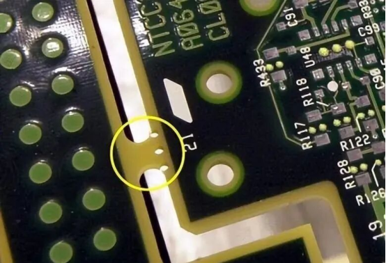
1.PCB Breakaway Tab (Mouse Bites)
During panelization, small connecting tabs with holes are left along the edges to hold boards together before separation. These holes resemble the perforations on postage stamps—hence the name “mouse bites” or “breakaway tabs.” They allow easy separation of individual PCBs after assembly.
2.PCB Via Types
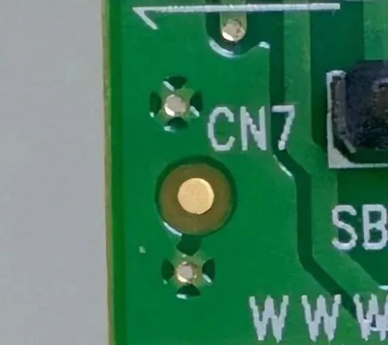
You’ll often see mounting holes surrounded by tiny vias. There are two main types of mounting holes: plated and non-plated. The surrounding vias serve two purposes:
Connecting the hole to internal layers (e.g., ground planes in multilayer PCBs).
Linking top and bottom pads in non-plated holes.

3.Solder Thief Pads
Wave soldering can sometimes cause solder bridges between SMD pins. To prevent this, an additional pad—2–3 times wider than the standard pad—is placed at the end of the pin. This “solder thief” absorbs excess solder and reduces bridging.

4.Fiducial Marks (Alignment Marks)
A fiducial mark consists of a small exposed copper circle inside a larger exposed circle. These marks serve as reference points for pick-and-place (PnP) machines during assembly. They are typically placed:
On the panel.
Near fine-pitch components (e.g., QFN, TQFP).
At the corners of the PCB.
5.Spark Gaps
Spark gaps provide basic protection against ESD, current surges, and overvoltage. When high voltage ionizes the air between two terminals, a spark forms, diverting energy away from sensitive circuits. While not highly reliable, they offer a low-cost safeguard. Breakdown voltage can be estimated using:
V = (3000 × p × d) + 1350,
where “p” is atmospheric pressure and “d” is the gap distance in millimeters.
6.PCB Conductive Keypads
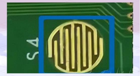
If you’ve opened a remote control or calculator, you’ve likely seen these. Conductive keypads consist of two interleaved—but not connected—terminals. Pressing a rubber button (with a conductive bottom) bridges the terminals, completing the circuit.
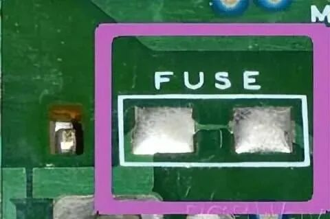
7.Fuse Traces
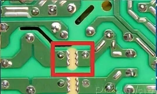
Similar to spark gaps, fuse traces are a budget-friendly protection method. A narrow “neck” in a power trace acts as a one-time fuse. This design can also serve as a PCB jumper—simply cut or etch the trace to disable a connection (found, for example, on some Arduino UNO reset lines).
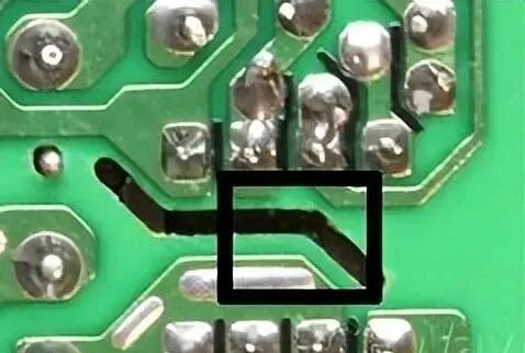
8.PCB Slotting (Creepage Slots)
In high-voltage PCBs (like power supplies), you may notice slots or grooves between traces. Repeated arcing can carbonize the board and cause short circuits. Adding slots in critical areas helps prevent carbon buildup, even if arcing occurs.
These markings enhance PCB functionality, reliability, and manufacturability. Understanding them helps in designing, assembling, and maintaining electronic devices efficiently.