


 Home
Home
How to Handle PCB Vias for a Perfect Balance of Performance and Cost?
 November 12,2025
Vias are the tiny but mighty heroes in multilayer PCBs, acting as vertical tunnels that connect different circuit layers. Believe it or not, drilling these small holes can eat up 30% to 40% of your total board manufacturing cost! So, designing them right is key.
Think of a via like a donut: it has a hole in the middle (the drill hole) and a ring around it (the pad). The size of both parts matters. Today's fast, compact electronics love small vias because they save precious wiring space and cause less signal interference. But there's a catch: the smaller the hole, the harder and more expensive it is to drill and coat it evenly with copper inside.
To help you nail the design, here are the core rules to follow, complete with notes for your upcoming images:
1.Standard Through-Hole Vias
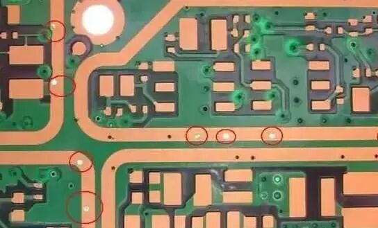
The most common type, these go through the entire board. A good rule of thumb is to keep the inner hole diameter at least 0.2mm (8mil) and the outer pad diameter at least 0.4mm (16mil). A handy formula is to make the outer diameter about double the inner one. For example, an 8mil hole often pairs with a 16mil pad.
2. BGA Area Strategies
Ball Grid Array (BGA) chips have pins underneath in a tight grid. For BGAs with 0.65mm spacing or larger, regular through-hole vias work fine. Using more complex buried or blind vias here is often overkill and costly. If you must use a blind via (which stops at an inner layer), a first-order type is best.
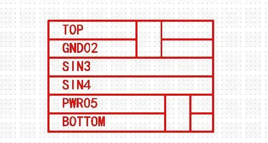
Figure 1: Example of a first-order blind via in a BGA region
3.Keep Vias Off Tiny Pads
It might seem convenient to place a via right on a component pad, but for small parts like 0402 resistors, this is risky. During soldering, the molten solder can get sucked into the via hole, leaving the component dry on one side and causing a defect called "tombstoning." It's safer to keep the via 4-8 mils away from the pad edge.

Figure 2: Recommended spacing between a via and a small component pad
4. Don't Crowd Your Vias
Vias need personal space. If they are placed too close together, the drill bit can break or wander into the neighboring hole during manufacturing, ruining both. A safe minimum distance is 0.5mm. Anything less than 0.3mm is a strict no-go.
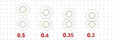
Figure 3: Diagram showing minimum via-to-via spacing
5. To Fill or Not to Fill? (Via Tenting)
For vias 0.5mm and smaller, it's standard practice to "tent" them—that is, cover them with solder mask. For even smaller holes, they are often filled with epoxy first and then covered. This is crucial in two cases: first, under metal shields to prevent shorts; second, under BGA chips to stop solder balls from bridging during assembly.

Figure 4: Via Application Scenarios
6. Locking Down Connector Pads
Heavy-use connectors like headphone jacks, power ports, or FPC cables endure physical stress. To prevent their pads from tearing off the board, it's smart to add 1-2 small vias directly in the large, fixed solder pads. This anchors the copper firmly to multiple layers.
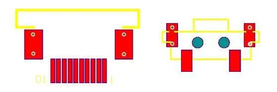
Figure 5: Via Placement in Fixed Pads
By sticking to these guidelines, you can design vias that make your PCB more reliable, better performing, and easier to manufacture without blowing your budget.