


 Home
Home
Why Do PCBAs Need a Process Edge?
 November 6,2025
When PCB designers create circuit boards, they often reserve a process edge. Have you ever wondered why this step is essential and what benefits it brings? Let’s break down the core reasons and value of designing a process edge for PCBA (Printed Circuit Board Assembly).
In PCBA design, reserving a process edge is a critical step to ensure smooth large-scale production and meet product quality standards. As a key link between design and manufacturing, proper process edge planning directly impacts the efficiency and stability of subsequent processes like Surface Mount Technology (SMT) and through-hole soldering. It has become essential knowledge for PCB designers worldwide.
1.What is a PCBA Process Edge?
A process edge (also called a working edge) is a narrow, blank strip along the PCB’s perimeter. It has no components, pads, or circuits—its sole purpose is to adapt to automated production equipment. It provides a stable clamping and conveying base for SMT pick-and-place machines, wave soldering equipment, and serves as a mounting area for panel fiducial marks (Mark points) to ensure precise optical positioning.
Per industry standards (e.g., IPC-A-610C), the process edge width must match production equipment requirements: a minimum of 5mm for standard PCBs, and 8mm or more for precision boards or special applications. The edge must be smooth (no gaps) with rounded corners to prevent jams during transportation.
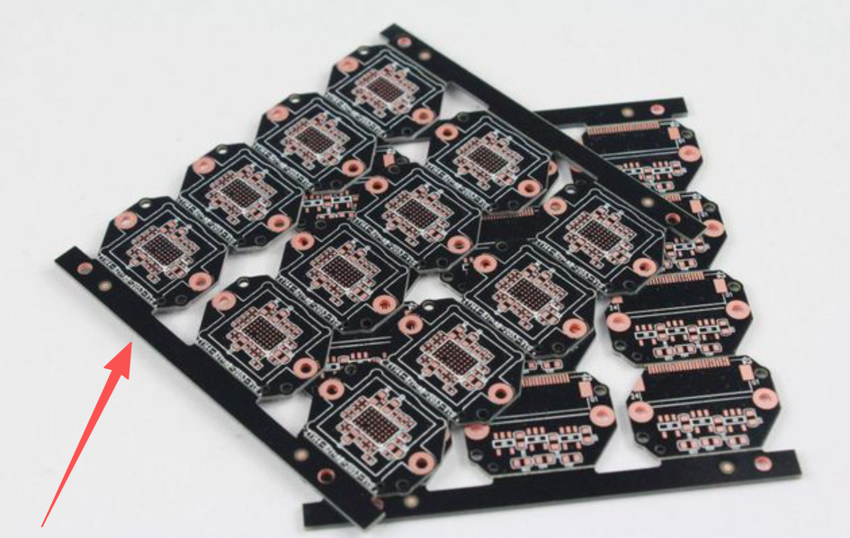
Picture: PCBA with Process Edge
2.Core Reasons to Design a Process Edge
Reserving a process edge isn’t an extra cost—it’s a proactive measure to mitigate production risks and boost overall efficiency, with three key benefits:
Supports SMT Production Line ConveyanceSMT assembly relies on equipment rails to transport and position PCBs. A process edge provides the necessary "grip area" for rail clamps. Without it (or with insufficient space), clamps can’t hold the board securely, leading to jams, position shifts, and poor soldering precision. For small or irregularly shaped PCBs, the process edge is indispensable—it extends the effective size to meet the minimum clamping requirements of automated equipment.
Protects Components from DamageDuring SMT pick-and-place operations, machine nozzles may collide with components near the PCB edge, causing damage or placement failures. A process edge creates a safe buffer zone. It also prevents interference between through-hole components and conveyor systems during wave soldering. Importantly, the process edge is not part of the final product and can be removed after assembly.
Enables Accurate Positioning and TestingFiducial marks (critical for SMT optical positioning) are typically placed on the process edge—they require at least 3mm of space from the board edge and a 5mm interference-free zone (no vias or test points). Additionally, test fixtures use the process edge to stabilize PCBs during ICT (In-Circuit Testing) and FCT (Functional Circuit Testing), ensuring precise contact between probes and test points for reliable results.
Process Edge: Key Benefits & Production Impacts
Key Benefit |
Direct Production Impact |
Supports SMT line conveyance |
Prevents jams/position shifts, ensures soldering precision |
Protects components from damage |
Reduces component loss, avoids placement/soldering failures |
Enables accurate positioning & testing |
Improves SMT positioning accuracy, reliable ICT/FCT test results |
3.Common Methods to Remove Process Edges
After assembly, the process edge is removed carefully to avoid damaging the PCB or components. Three widely used methods:
Router Cutting: Uses high-speed milling cutters for smooth, precise cuts with minimal mechanical stress. Ideal for complex shapes and high-volume production, though equipment costs are higher.
V-Cut Cutting: Separates the edge along pre-cut V-grooves. Cost-effective, fast, and dust-free, but only suitable for straight cuts and requires precise groove depth matching the PCB thickness.
Manual Removal: Uses pliers or hand folding for small-batch trials or simple PCBs. Low-cost but risky—may cause microcracks or solder joint damage. Stamp holes (3-5 holes, ≤0.8mm diameter) help concentrate stress and reduce harm.
4.Conclusion
Process edge design and removal reflect the Design for Manufacturability (DFM) principle. From width selection and fiducial mark placement to removal method choice, every step balances design standards with production reality. A well-designed process edge avoids automation issues, protects components, and lowers costs—making it foundational to consistent PCBA quality and efficiency.