


 Home
Home
Do Fewer PCB Layers Mean Lower Costs?
 December 19,2025
In electronic design, a common strategy to reduce costs is to minimize the number of PCB layers. While this approach can lower manufacturing expenses and simplify routing in some cases, it may be counterproductive under specific conditions. Furthermore, the industry overwhelmingly favors even-layer PCBs over odd-layer configurations. This article examines why reducing layers is not always the optimal choice and explains the technical and economic reasons behind the preference for even-layer designs.
1.Why Reducing Layers Isn’t Always the Best Choice
Although fewer PCB layers can reduce upfront manufacturing costs, this approach may introduce challenges that compromise performance, reliability, and long-term value. For high-density designs, reducing layers can severely limit routing space, potentially forcing the use of longer traces, additional vias, or layout compromises—all of which can degrade signal integrity. Moreover, fewer ground and power planes reduce shielding effectiveness, increasing the risk of electromagnetic interference (EMI). Thermal management also becomes more difficult with fewer internal copper layers to dissipate heat, which may affect component longevity. In high-speed designs, maintaining consistent impedance control is more challenging without dedicated signal-reference plane pairs. Additionally, highly dense 2- or 4-layer boards may require finer traces and tighter tolerances, which can offset initial savings by increasing manufacturing complexity and cost.
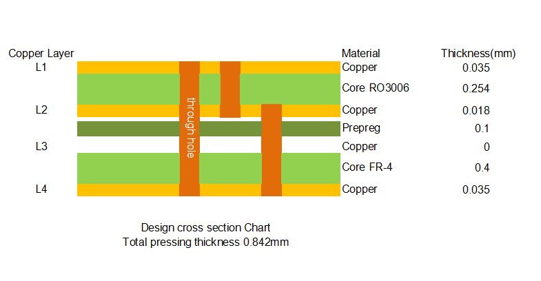
3-layer RO3006 and FR4 PCB STACKUP
2.Why Are Most PCBs Made with Even Layers?
The industry's strong preference for even-layer PCBs is rooted in manufacturing efficiency, cost predictability, and reliability. The following table compares the key characteristics of even-layer and odd-layer PCB designs:
Aspect |
Even-Layer PCB |
Odd-Layer PCB |
Impact & Consideration |
Raw Material Cost |
Standard symmetrical structure |
Slightly lower due to one less dielectric and copper layer |
Material cost difference is typically less than 5% of total cost, making it a minor factor in decision-making. |
Manufacturing Process |
Standard symmetrical lamination process |
Requires non-standard asymmetric lamination or addition of a dummy core |
Non-standard processes increase complexity, alignment difficulty, and production time. |
Warpage Risk |
Low (balanced copper distribution and symmetrical thermal stress) |
High (asymmetric structure leads to uneven lamination tension during cooling) |
Warpage can affect SMT placement accuracy, solder joint reliability, and long-term mechanical stability. |
Production Efficiency & Yield |
High (optimized production lines and mature processes) |
Lower (non-standard handling increases risks of scratches, misalignment, and errors) |
Yield differences may increase total cost, offsetting any savings from reduced material use. |
Design Flexibility |
Enables optimized stack-up for signal integrity, power distribution, and EMC performance |
Requires structural balancing through blank layers or adjusted dielectric thickness |
Even-layer designs more easily support optimized routing, impedance control, and EMI mitigation. |
Typical Applications |
Used in the vast majority of scenarios: consumer electronics, industrial controls, high-speed designs, etc. |
Only used in special cases with strict constraints on size or layer count |
Even-layer designs are recommended unless there is a mandatory requirement for an odd-layer board. |
As the table illustrates, even-layer PCBs offer significant advantages in manufacturing efficiency, quality control, and long-term reliability. While odd-layer PCBs may save a small amount of raw material, the increased process complexity, yield risks, and potential quality issues often lead to higher total costs. This is especially true for applications involving high-density interconnect (HDI), high-speed circuits, or stringent thermal management requirements, where the symmetrical structure of even-layer designs provides a more reliable foundation for signal and power integrity.
3.Cost Optimization Without Sacrificing Performance
To optimize PCB costs effectively, consider the following strategies: First, evaluate whether a well-designed 4-layer board can fulfill the requirements of a moderate-speed application that might otherwise use 6 layers, as this can reduce costs while maintaining adequate signal integrity. Second, consider adopting HDI technology—although the per-layer cost may be higher, it can reduce the total layer count and overall board size, resulting in net savings. Third, ensure stack-up symmetry in even-layer designs to prevent warpage, a critical factor in lead-free soldering processes. Finally, optimize the use of power and ground planes by carefully partitioning them to serve multiple voltage domains within a single layer, though this requires meticulous management of return paths.
4.Conclusion
While reducing the number of PCB layers can lower direct manufacturing costs, it is not always the most cost-effective approach when considering overall system performance, reliability, and compliance. Even-layer PCBs remain the industry standard due to their advantages in manufacturing efficiency, lower warpage risk, and better cost-to-reliability ratio. When design constraints necessitate an odd-layer stack-up, balancing techniques such as adding non-functional layers or adjusting dielectric thickness can help mitigate drawbacks—but these measures often negate the marginal material savings. Therefore, a holistic perspective that considers cost, manufacturability, and performance is essential for selecting the optimal PCB layer count and configuration.
Founded in 2003, Shenzhen Bicheng Electronics Technology Co., Ltd is an established high frequency PCB supplier and exporter in Shenzhen, China, serving customers worldwide.
We are devoted to delivering high-frequency PCB products and solutions of the highest quality, along with customized service. Get in touch with us to start your project !
Visit https://www.bicheng-enterprise.com to learn more.
Contact Vicky at v.xie@BTL_VickyXie.com to unlock its full potential.