


 Home
Home
What is DFM for PCB? Common DFM Issues to Avoid
 September 21,2026
Many electronic engineers finish PCB design and export Gerber files directly for manufacturing. However, many seemingly correct layouts contain hidden manufacturability risks that lead to short circuits, open circuits, low yield rates, assembly failures, and delayed project delivery. These problems are mostly avoidable with a standard PCB DFM check before production.
Design for Manufacturability (DFM) is the most critical pre-production step that bridges PCB design and PCB manufacturing. It helps identify layout details that do not match industrial process capabilities, ensuring stable production, consistent quality, and cost-effective mass production.
1. PCB DFM Overview: Standard vs. Risky Design
The table below summarizes the most common DFM inspection items, standard requirements, and typical design issues, suitable for documentation and project review.
Inspection Item |
Standard DFM Requirement |
Common DFM Issues & Risks |
Trace Width & Spacing |
Meet minimum factory line width and clearance limits |
Too thin traces, insufficient spacing causing short/open circuits |
Via Annular Ring |
Maintain sufficient copper ring around drill holes |
Tiny annular ring leading to hole breakout and broken circuits |
Pad Size & Shape |
Pad dimensions fit soldering and processing tolerance |
Undersized pads causing SMT assembly soldering failure |
Solder Mask Design |
Clear isolation between adjacent conductive areas |
Solder mask bridging, exposed copper crosstalk risks |
Copper Distribution |
Balanced copper density on all layers |
Uneven copper causing board warpage and lamination defects |
Board Outline & Slots |
Smooth routing structure without sharp dead angles |
Sharp inner angles resulting in copper cracking during fabrication |
2. What is PCB DFM (Design for Manufacturability)?
PCB DFM refers to the process of checking and optimizing PCB layout files based on standardized manufacturing processes. It evaluates whether trace width, spacing, vias, pads, copper layout, and board structure can be produced stably in mass production.
A perfect circuit simulation result does not guarantee a manufacturable PCB. Many design practices work theoretically but cannot withstand actual etching, drilling, lamination, and surface finishing processes. DFM review eliminates these inconsistencies in advance.
Professional PCB DFM focuses on three core goals:
- Ensure 100% manufacturable PCB layout
- Improve production yield and reduce defective rates
- Avoid repeated revision costs and shorten project lead time
3. Most Common PCB DFM Issues Found in Production
3.1 Insufficient trace width and clearance
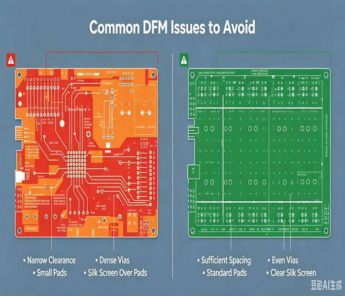
Trace width and spacing are the most basic DFM parameters. When layout lines are too narrow or gaps between lines are too small, the etching process may cause residual copper or line breakage, resulting in short circuits or open circuits. This is the top cause of PCB production failure.
3.2 Undersized via annular ring
The annular ring is the copper area surrounding a drilled via. If the ring is too small, mechanical drilling deviation will break the copper connection, causing hidden open-circuit failures. This issue cannot be detected by electrical testing in the design stage.
3.3 Unqualified pad dimensions
Too small or irregular pads affect solder adhesion during SMT assembly. Even if bare PCBs are produced normally, poor pad design will lead to insufficient solder, virtual soldering, and component falling off after assembly.
3.4 Unbalanced copper layer distribution
Multilayer PCBs with extremely uneven copper density suffer from inconsistent thermal expansion and lamination pressure. This commonly causes board warpage, layer offset, and delamination, especially for thin PCBs and high-frequency boards.
3.5 Unreasonable silkscreen layout
Silkscreen text overlapping pads or traces is a frequent design oversight. Silkscreen ink covering pad areas directly blocks soldering points and leads to assembly defects.
4. Consequences of Skipping DFM Inspection
Ignoring DFM checking before mass production often causes predictable project losses:
- Production suspension due to unmanufacturable design parameters
- High defective rate and low PCB yield
- Repeated design revisions and remanufacturing, delaying product launch
- Hidden reliability problems appearing after assembly and shipment
5. Standard PCB Workflow with DFM Optimization
To achieve high yield, stable quality, and fast delivery, all custom PCB projects should follow the standard process:
Complete PCB Design → Gerber File Export → Professional DFM Review → Design Optimization → Precision PCB Manufacturing → Full Quality Testing
DFM optimization ensures the design matches industrial manufacturing standards, making prototypes and batch production more stable and cost-efficient.
6. Conclusion
PCB DFM is an essential standard procedure between design and manufacturing. It transforms theoretical circuit design into industrial producible design. Reasonable DFM checking effectively avoids most common PCB defects, improves production consistency, and reduces overall project costs.
For any custom PCB project, a complete DFM review is the simplest and most efficient way to improve yield and avoid technical risks.
Professional PCB Manufacturing & DFM Review Service
We provide professional PCB pre-production DFM analysis and high-precision PCB fabrication services. Covering single-layer, double-layer, multilayer, and high-frequency PCBs, our standardized manufacturing and strict quality testing ensure stable board quality for prototypes and mass production. If you have finished Gerber files, feel free to contact us for detailed DFM evaluation and quotation.