


 Home
Home
Bare PCB vs Assembled PCB: What’s The Difference?
 September 23,2026
When developing and sourcing electronic hardware, design engineers, project managers, and procurement professionals frequently encounter two core circuit board types: bare PCB and assembled PCB (PCBA). Many new industry buyers mistakenly treat them as interchangeable products, leading to incorrect ordering, mismatched project schedules, and unnecessary budget waste. In fact, bare PCBs and assembled PCBs belong to two completely different stages of electronic manufacturing, with distinct structural features, production processes, functional attributes, and application boundaries. Fully understanding their core differences allows engineering teams to select the correct board type according to project progress, accurately arrange R&D debugging and mass production plans, and effectively control overall project costs.
As a professional manufacturer focusing exclusively on bare PCB fabrication, we have received numerous consulting requests from global clients regarding the differences between blank bare circuit boards and component-assembled PCBs. Many customers are unclear about which board type suits prototype testing, small-batch verification, or formal mass production. This article systematically elaborates on the professional definitions, production procedures, functional characteristics, typical application scenarios, and practical selection guidelines of bare PCB and assembled PCB based on industrial manufacturing standards, providing reliable technical references for electronic project development and supplier cooperation.
1. Quick Comparison: Bare PCB vs Assembled PCB
The table below summarizes the key differences between bare PCB and assembled PCB. It is concise, standardized, and fully compatible with one-click copying to Word for project documentation and supplier evaluation.
Comparison Item |
Bare PCB |
Assembled PCB (PCBA) |
Basic Definition |
Pure circuit substrate without any electronic components soldered |
Finished board with all electronic components soldered and mounted |
Core Status |
Empty circuit board, only conductive traces and pads |
Functional circuit board with complete hardware configuration |
Function Performance |
No electrical functions, cannot work independently |
Complete circuit functions, ready for direct device use |
Main Process |
Substrate fabrication, etching, drilling, surface finishing, testing |
Bare PCB production + SMT mounting + DIP soldering + functional testing |
Application Scenarios |
Independent component assembly, secondary development, batch spare boards |
Product prototyping, finished electronic equipment, direct mass delivery |
Cost & Lead Time |
Lower cost, shorter production cycle |
Higher total cost, longer lead time due to component procurement and soldering |
2. What Is a Bare PCB?
A bare PCB, also widely known as a blank printed circuit board, is the most fundamental hardware carrier in the electronics industry. It is manufactured through a complete set of standardized precision processes, including substrate cutting, circuit pattern etching, mechanical and laser drilling, inner layer alignment, lamination, solder mask coating, surface finishing, and strict factory quality testing. The finished bare PCB only retains preset conductive copper traces, insulated substrate layers, conductive vias, and soldering pads, with no electronic components mounted or soldered on the board surface.
Essentially, a bare PCB is a pure structural and conductive carrier without any independent electrical working functions. It cannot be powered on, run programs, or implement any circuit logic functions alone. However, its manufacturing accuracy, circuit stability, insulation performance, and structural durability directly determine the assembly quality and long-term operational reliability of subsequent electronic products. For high-frequency wireless applications, engineers often select TP450 2-Layer 2.5mm Bare Copper PCB for RF and microwave performance. All finished electronic equipment, whether consumer electronics, industrial control devices, automotive modules, or communication equipment, relies on high-quality bare PCBs as the core foundation.
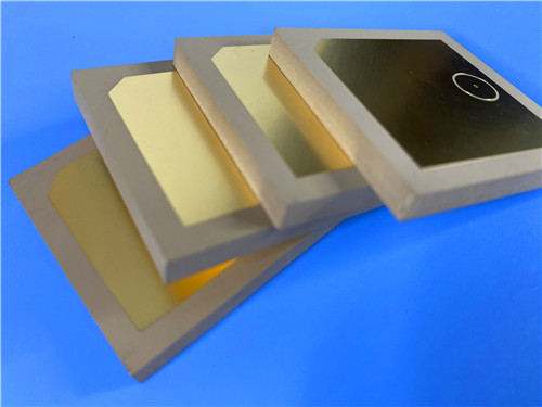
Common use cases for bare PCB:
- Engineers complete independent component matching and secondary assembly
- Project trial testing with flexible component replacement
- Reserve batch spare boards for later maintenance and upgrade
- Custom personalized component layout and debugging
3. What Is an Assembled PCB (PCBA)?
Assembled PCB, commonly referred to as PCBA (Printed Circuit Board Assembly), is a finished functional circuit board formed by secondary processing on the basis of qualified bare PCBs. The complete PCBA manufacturing workflow includes electronic component procurement, material verification, SMT surface mount soldering, DIP through-hole plug-in processing, reflow soldering, wave soldering, solder joint inspection, and overall functional aging testing.
Different from blank bare PCBs that only retain circuit structures, assembled PCBs integrate complete electronic components such as chips, resistors, capacitors, inductors, and connectors. After program burning and strict functional calibration, PCBA can realize complete signal transmission, data processing, power supply control, and other core functions. It is the final functional module directly applied to finished electronic products and can be installed and put into use after simple peripheral matching.

Common use cases for assembled PCB (PCBA):
- Official prototype verification and function confirmation
- Formal mass production of consumer electronics, industrial control, and automotive products
- Finished circuit modules that require no secondary processing
- Cross-industry finished board customization and direct delivery
4. Core Differences in Practical Projects
4.1 Functional Difference
The most essential difference between the two lies in functional implementation. A bare PCB is merely a standardized circuit carrier with fixed trace distribution and via positions. It only provides conductive channels and structural support, and cannot implement any circuit logic or equipment functions independently. All functional realization depends on subsequent manual or automated component assembly and debugging. In contrast, an assembled PCB completes component mounting and soldering based on bare PCB substrates, forming a complete and executable circuit system. It can directly respond to power supply signals and data instructions, fully meeting the functional operation requirements of terminal electronic equipment.
4.2 Processing & Workflow Difference
In terms of production procedures and technical thresholds, bare PCB manufacturing focuses on precision substrate processing, circuit etching consistency, drilling accuracy, lamination flatness, and surface finish quality. The process flow is mature and standardized, with stable batch yield and controllable quality risks. Assembled PCB production is a complex secondary manufacturing process based on qualified bare PCBs. It involves component screening and compatibility verification, high-precision tin printing, automatic optical inspection of solder joints, reflow temperature curve control, and long-term functional aging tests. The overall process is more cumbersome, with higher technical requirements for production environment and equipment, and stricter quality control standards.
4.3 Cost & Cycle Difference
There are obvious differences in comprehensive cost and delivery cycle between the two products. Bare PCB only involves substrate materials, manufacturing processes, and quality testing links, with low unit production cost and short delivery cycle. It is highly suitable for rapid iteration and repeated debugging in the early R&D stage of electronic projects. Assembled PCBs require additional component procurement, inventory management, manual or machine soldering, and multi-round functional testing on the basis of bare PCB production. Component price fluctuations, material lead times, and soldering yield rates will all affect the overall cost and delivery time. Therefore, the comprehensive cost of PCBA is much higher, and the production cycle is relatively longer, but it can save customers a large amount of subsequent assembly labor costs and debugging time costs.
4.4 Applicable Crowd Difference
Their applicable customer groups and project stages are also clearly differentiated. For R&D teams, startup teams, and technical departments that need frequent circuit debugging, parameter modification, and component replacement in the early stage of product development, bare PCBs are the most cost-effective choice. Customers can flexibly match components and adjust assembly schemes according to test data to optimize product performance. For mature electronic manufacturers, batch order suppliers, and projects with fixed and finalized technical solutions, assembled PCBs are more efficient and practical. It can realize one-stop finished product procurement, shorten the overall product launch cycle, and facilitate standardized batch delivery.
5. How to Choose Between Bare PCB and Assembled PCB?
To help global clients avoid ordering errors and optimize project resource allocation, we summarize clear selection principles based on project development stages and actual demand scenarios:
- Choose Bare PCB: In the early R&D stage, frequent circuit debugging, uncertain component parameters, and independent assembly requirements
- Choose Assembled PCB: Mature project solutions, batch mass production, finished product delivery, and one-stop procurement requirements
6. Conclusion
Bare PCB is the basic empty circuit substrate of all electronic products, undertaking the core functions of circuit conduction and structural support. Its manufacturing quality determines the stability and durability of electronic products fundamentally. Assembled PCB is the finished functional circuit board processed on the basis of bare PCB, focusing on realizing complete product functions and terminal application value. The two are closely connected but have clear boundaries in terms of production links, product attributes, and application scenarios, corresponding to the R&D debugging stage and mass production delivery stage of electronic projects respectively.
Clarifying the essential differences between bare PCB and PCBA enables engineers and purchasers to accurately match product types according to project progress, effectively avoid resource waste and order mistakes, reasonably control R&D and production costs, and greatly optimize the overall progress and quality management of electronic product development.
Professional Bare PCB Manufacturing Service
We focus purely on high-quality bare PCB fabrication for global clients, without providing PCB assembly services. We support customized production of single-layer, double-layer, multi-layer, high-frequency, and impedance-controlled bare PCBs, covering prototype trial production, small-batch verification, and large-scale mass production. All bare PCB products undergo strict visual inspection, AOI optical detection, and professional electrical performance testing to ensure precise production restoration, stable batch consistency, and qualified yield rate. If you have finished Gerber files and customized bare PCB procurement demands, contact our professional team to obtain a detailed technical evaluation and competitive quotation.