

 Home
-
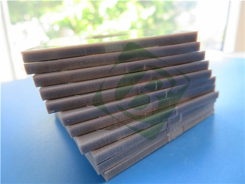
Newly shipped PCBs
-
TP450 2-Layer PCB 2.5mm Thick Bare Copper low loss Laminate for superior RF and microwave performance
Home
-
Newly shipped PCBs
-
TP450 2-Layer PCB 2.5mm Thick Bare Copper low loss Laminate for superior RF and microwave performance
TP450 2-Layer PCB 2.5mm Thick Bare Copper low loss Laminate for superior RF and microwave performance
Printed Circuit Boards are custom-made products; the images and specifications provided are for reference only.
1.Introduction of TP series
TP material is a high-frequency laminate known for its unique ceramic and Polyphenylene Oxide (PPO) resin dielectric layer, which omits traditional fiberglass reinforcement. This composition allows for precise control over the dielectric constant (Dk), which can be tailored from 3.0 to 25.0 to meet specific circuit design needs. The material offers excellent dielectric stability, low loss, and high reliability.
The product naming convention indicates the copper cladding: bare substrate (TP), single-sided cladding (TP-1), and double-sided cladding (TP-2). Standard Dk values, such as 3.0, 6.15, and 10.2, correspond to part numbers like TP300, TP615, and TP1020, respectively.
2. Features (TP450 PCB)
- Dielectric constant (Dk) of 4.5±0.2 at 10GHz
- Dissipation factor of .0010 at 10GHz
- Low TCDK at -50 ppm/°C, -55°C to 150°C
- CTE x-axis of 50 ppm/°C, CTE y-axis of 50 ppm/°C, CTE z-axis of 60 ppm/°C, -55°C to 150°C
- Thermal conductivity of 0.44 W/mk
- Moisture absorption of 0.01%
- UL 94-V0
3. PCB Construction details:
-Base material: TP450
- Layer count: Double sided
- Board dimensions: 121mm x 125 mm=1PCS, +/- 0.15mm
- Minimum Trace/Space: 6/4 mils
- Minimum Hole Size: 0.5mm
- No Blind vias.
- Finished board thickness: 2.6mm
- Finished Cu weight: 1oz (1.4 mils) outer layers
- Via plating thickness: 20 μm
- Surface finish: Electroless Nickel Immersion Gold (ENIG)
- Top Silkscreen: No
- Bottom Silkscreen: No
- Top Solder Mask: No
- Bottom Solder Mask: No
- 100% Electrical test used prior to shipment
4. PCB Stackup: 2-layer rigid PCB
Copper_layer_1 - 35 μm
TP450 Core - 2.54 mm (100mil)
Copper_layer_2 - 35 μm
5.PCB Statistics:
Components: 23
Total Pads: 80
Thru Hole Pads: 56
Top SMT Pads: 24
Bottom SMT Pads: 0
Vias: 93
Nets: 2
6. Type of artwork supplied: Gerber RS-274-X
7. Quality standard: IPC-Class-2
8. Availability: worldwide
9. Some Typical Applications:
- Global Satellite Navigation System
- missile-borne,
- fuze technology
- miniaturized antenna