


 Home
-
Blog
-
Can Your PCB Handle 10 oz Copper on 8 Layers? TU-865 PCB Solves the Heavy Copper Challenge
Home
-
Blog
-
Can Your PCB Handle 10 oz Copper on 8 Layers? TU-865 PCB Solves the Heavy Copper Challenge
Can Your PCB Handle 10 oz Copper on 8 Layers? TU-865 PCB Solves the Heavy Copper Challenge
 May 20,2026
When a customer asks for 10 oz copper on all eight layers, you know the application is serious.
Most PCBs run on 1 oz or 2 oz copper. Even power supply boards rarely go above 4 oz. But every so often, a project comes across the desk that demands something else—something that handles 50, 80, or even 100 amps per layer without turning into a heating element.
This is one of those projects.
1. Why 10 oz Copper?
Standard copper weights are measured in ounces per square foot. One ounce equals approximately 35µm of thickness. At 10 oz, each copper layer is 350µm thick—roughly ten times thicker than a typical signal layer.
Why would a design need this much copper? Two reasons.
First, current carrying capacity. A 1 oz trace at 10mm width carries about 5-6 amps before temperature rise becomes a concern. A 10 oz trace of the same width carries roughly 10 times that. For power distribution in electric vehicle systems or industrial motor drives, heavy copper is often the only practical solution.
Second, thermal management. Thick copper acts as a heat spreader. It pulls heat away from power components and distributes it across the board, reducing hot spots and improving reliability.
The trade-off? Fabrication complexity. For a Heavy copper PCB, the thick copper does not etch like standard copper. It requires slower etch speeds, different chemistry, and careful compensation for undercut. Not every PCB shop can do it.
2. Material Choice: TU-865 Laminate
With 10 oz copper, the board will go through multiple lamination cycles and extended etch processes. The dielectric material must survive that without warping or delaminating.
Property |
TU-865 Value |
Why It Matters |
Tg |
200°C |
Withstands lead-free reflow without softening |
Flammability |
UL94V-0 |
Required for most industrial and automotive applications |
Halogen Content |
Free |
Meets environmental regulations |
Max Operating Temp |
130°C |
UL-rated continuous use |
TU-865 is a halogen-free FR4-type material rated for harsh environments. The high Tg of 200°C is critical here—standard FR4 (Tg 135-170°C) may soften or warp under the thermal stress of heavy copper processing.
TU-865P is the prepreg specifically designed for use with TU-865 laminate. It shares the same halogen-free, high-Tg characteristics and is available in multiple glass styles including 106, 1080, 2113, 2116, 1506, and 7628.
TU-865 laminate also offers anti-CAF (conductive anodic filament) resistance, which matters for boards that will operate in humid or high-voltage environments.
3. Stack-Up Overview
3. Stack-Up Overview
This 8-layer heavy copper PCB uses a TU-865 core (0.4mm) with standard prepreg layers. The total pressed thickness is 4.4mm, with 1 oz (0.35mm) heavy copper on all eight layers.
At 4.4mm thick with 1 oz copper, registration during lamination is a key challenge. Copper expands differently than the dielectric material, which can cause inner layer shifting and via misalignment without proper compensation. Our process addresses this by adjusting artwork scaling for each layer based on copper percentage and distribution, ensuring precise alignment even with heavy copper.
4. Via Construction: Blind, Buried, and Through Hole
This board requires three types of vias:
Blind vias: Connect outer layers (GTL/GBL) to inner layers
Buried vias: Connect inner layers only
Through holes: Connect all layers from top to bottom
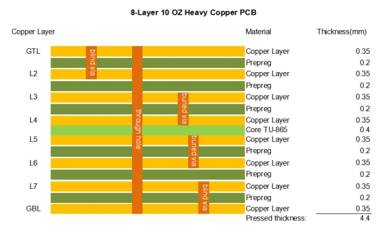
Additionally, all vias are filled with conductive copper paste.
Via Type |
Description |
Blind Vias |
Connect outer layers to inner layers, reducing the effective via depth |
Buried Vias |
Connect inner layers only, not visible from the outer surface |
Through Holes |
Full-depth vias connecting all 8 layers |
Conductive Paste Fill |
All vias are filled with conductive copper paste, maintaining low impedance and supporting heavy copper plating |
Unlike standard epoxy plugging, conductive copper paste fill keeps vias low-impedance while creating a flat surface for heavy copper layers—key for reliable high-current performance.
For this 4.4mm thick PCB, we use optimized plating parameters to ensure full, uniform copper coverage even on blind vias with aspect ratios exceeding 10:1.
5. Surface Finish and Solder Mask
Surface finish is Immersion Gold (ENIG) . For heavy copper boards, ENIG provides a flat, solderable surface that does not require additional copper thickness. The nickel layer (3-6µm) acts as a barrier, while the thin gold layer (0.05-0.1µm) protects against oxidation.
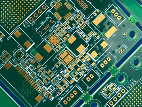
Solder mask is green on both sides, with white legend ink. At 4.5mm thick, applying solder mask evenly over the 10 oz copper features requires multiple passes or a specialized spray coating system. Standard curtain coating may leave thin spots on the vertical edges of thick copper traces.
6. Applications and Limitations
Typical applications include automotive power distribution modules, industrial motor drives, server backplanes with high current requirements, and telecom base station power amplifiers.
However, there is a limitation to note. TU-865 has a maximum operating temperature of 130°C (UL rating). This is the continuous use temperature, not the peak assembly temperature. If the end application requires sustained operation above 130°C, a different material (polyimide or high-Tg PTFE) would be necessary.
For applications that stay within that limit, TU-865 provides a reliable, halogen-free solution with excellent moisture resistance and thermal cycling survival.
7. Summary
This 8-layer, 10 oz copper PCB is a specialist product. It is designed for high-current, thermally demanding environments where standard FR4 and standard copper weights would fail. If your design requires heavy copper and a material that can handle the thermal stress of processing and operation, this is a configuration we have successfully delivered.