

 Home
-
Newly shipped PCBs
-
TF600 25mil Double-Layer High Frequency PCB - Low Loss, High Stability TF600 Laminate From WangLing for RF and Microwave Applications
Home
-
Newly shipped PCBs
-
TF600 25mil Double-Layer High Frequency PCB - Low Loss, High Stability TF600 Laminate From WangLing for RF and Microwave Applications
TF600 25mil Double-Layer High Frequency PCB - Low Loss, High Stability TF600 Laminate From WangLing for RF and Microwave Applications
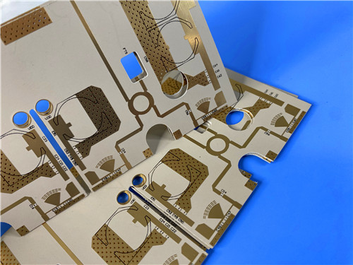
Printed Circuit Boards are custom-made products; the images and specifications provided are for reference only.
1.TF600 2-Layer High Frequency PCB Introduction
WangLing TF600 2-Layer High Frequency PCB is a high-reliability rigid printed circuit board manufactured with TF600 laminate, designed to meet the strict requirements of RF/microwave applications. Constructed with a 2-layer rigid structure and 0.7mm finished thickness, this PCB integrates the excellent performance of TF600 laminate—including ultra-low dielectric loss, stable DK consistency, and FR4-compatible processing—with precise manufacturing standards. It supports 260℃ lead-free assembly and features outstanding thermal stability and moisture resistance, making it a reliable choice for high-frequency designs where low insertion loss and signal integrity are critical. Without glass fiber cloth, TF600 PCB minimizes signal interference and ensures consistent performance across a wide frequency range, suitable for global industrial and commercial applications.
2. PCB Features
- Board Structure: 2-layer rigid PCB, with a finished thickness of 0.7mm for compact and stable installation.
- Core Material: TF600laminate (0.635mm/25mil), modified PTFE resin with micron-sized ceramic fillers, no glass fiber cloth.
- Copper Specifications: 1oz (1.4 mils) finished copper weight on outer layers (35μm per layer), 20μm via plating thickness for reliable conductivity.
- Precision Parameters: Minimum trace/space of 5/6 mils, minimum hole size of 0.35mm, no blind vias, ensuring precise circuit routing.
- Surface & Silkscreen: ENIG surface finish for excellent solderability and corrosion resistance; black top silkscreen for clear component identification, no bottom silkscreen.
- Special Process: Copper filling vias on designated IC pads, enhancing connection reliability and heat dissipation.
- Quality Control: 100% electrical test prior to shipment, complying with IPC-Class-2 standards for consistent quality.
- Dielectric Performance: DK of 6.0 ± 0.15 at 10GHz, Df of 0.0025 at 10GHz, ensuring optimal signal integrity.
- Thermal & Mechanical Stability: Tg >280℃ (DSC), T260 >60 minutes, T288 >20 minutes; UL 94-V0 flammability rating; high CAF and chemical corrosion resistance.
3. PCB Benefits
- Superior Signal Integrity: Ultra-low dielectric loss (Df=0.0025 at 10GHz) and stable DK consistency minimize signal attenuation and distortion, ideal for high-frequency RF/microwave applications.
- Easy Manufacturing: FR4-compatible processing (drilling, plating, lamination) reduces production complexity and costs, ensuring efficient mass production.
- Lead-Free Compliance: Supports 260℃ lead-free assembly, meeting global environmental and industry standards for electronic products.
- High Reliability: Low moisture absorption (max. 0.06%), excellent thermal stability, and high peel strength (min. 0.80 N/mm) ensure long-term performance in harsh environments.
- Dimensional Stability: CTE values of X=14-16 ppm/℃, Y=12-14 ppm/℃, Z=40-45 ppm/℃ prevent board warpage during assembly and operation.
- Cost-Effective: 2-layer structure balances performance and cost, suitable for medium-complexity high-frequency circuit designs without sacrificing reliability.
- Global Availability: Accessible worldwide, ensuring timely supply and support for international projects and customers.
- Precise Circuit Performance: Copper filling vias on designated IC pads and 100% electrical testing guarantee consistent and reliable circuit connections.
4. PCB Construction Details
Construction Item |
Specifications |
Board Dimensions |
78mm x 65mm = 1PCS, +/- 0.15mm |
Minimum Trace/Space |
5/6 mils |
Minimum Hole Size |
0.35mm |
Blind Vias |
No |
Finished Board Thickness |
0.7mm |
Finished Cu Weight (Outer Layers) |
1oz (1.4 mils) |
Via Plating Thickness |
20 μm |
Surface Finish |
ENIG |
Top Silkscreen |
Black |
Bottom Silkscreen |
No |
Top Solder Mask |
No |
Bottom Solder Mask |
No |
Special Process |
Copper filling vias on designated IC Pad |
Quality Test |
100% Electrical test used prior to shipment |
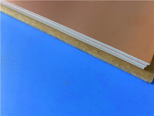
5. PCB Stackup
2-layer rigid PCB, with the following stackup structure (from top to bottom):
- Copper_layer_1: 35 μm
- TF600 Laminate: 0.635 mm (25mil)
- Copper_layer_2: 35 μm
6. PCB Statistics
- Components: 43
- Total Pads: 61
- Thru Hole Pads: 32
- Top SMT Pads: 29
- Bottom SMT Pads: 0
- Vias: 34
- Nets: 2
7. Type of Artwork Supplied
Gerber RS-274-X
8. Accepted Standard
IPC-Class-2
9. Availability
Worldwide
10. Typical Applications
- Microwave/RF Transceivers
- 5G/6G Massive MIMO Antennas
- Radar Systems (Automotive ADAS, Aerospace)
- Satellite Communication Payloads
- High-Power RF Amplifiers
- Test & Measurement Equipment (Vector Network Analyzers)
11. TF600 Copper Clad Laminate Overview
TF600 is a high-performance thermosetting high-frequency laminate, composed of modified Polytetrafluoroethylene (PTFE) resin and micron-sized ceramic fillers. It is designed without glass fiber cloth, enabling precise adjustment of dielectric constant (DK) by modifying the ratio of ceramic to PTFE resin.
12. Key Features of TF600 laminate
- Stable dielectric constant (DK) ranging from 3.0 to 16.0, with common values including 3.0, 6.0, 9.2, 9.6, 10.2, and 16.0, paired with low dielectric loss for superior signal integrity.
- Ideal for microwave and millimeter-wave PCB fabrication, supporting high-frequency signal transmission without significant loss.
- Superior thermal performance: long-term operating temperature ranges from -80℃ to +200℃, higher than TP series materials.
- Flexible thickness options: 0.635mm to 2.5mm, adaptable to various PCB design requirements.
- Radiation resistant and low outgassing, suitable for harsh environment applications such as aerospace and automotive ADAS.
- Easy processing compatibility: can be fabricated using standard thermoplastic material processing methods, reducing manufacturing complexity and cost.
13. TF600 CCL Product Classification
- TF: Bare laminate without copper cladding, suitable for custom copper cladding processes.
- TF-1: Single-sided copper-clad laminate, cost-effective for simple circuit designs.
- TF-2: Double-sided copper-clad laminate, ideal for double-layer PCB fabrication requiring interlayer connections.
14. Summary
- TF600 2-Layer High Frequency PCB is a high-performance, reliable printed circuit board engineered for RF/microwave applications that demand low signal loss, stable dielectric performance, and long-term durability.
- Leveraging the superior properties of TF600 laminate, this 2-layer, 0.7mm thick PCB delivers consistent electrical performance, easy manufacturing compatibility, and compliance with global industry standards.
- It is designed to meet the needs of diverse high-frequency applications—from 5G/6G antennas to aerospace radar systems—providing customers worldwide with a cost-effective and high-reliability solution for their high-frequency PCB requirements.