

 Home
-
Newly shipped PCBs
-
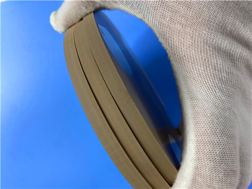
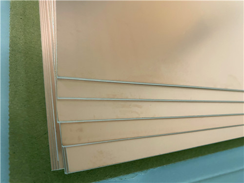
6mm TP2000 High DK PCB--2-Layer RF and Microwave Printed Circuit Board with Pure Gold
Home
-
Newly shipped PCBs
-
6mm TP2000 High DK PCB--2-Layer RF and Microwave Printed Circuit Board with Pure Gold
6mm TP2000 High DK PCB--2-Layer RF and Microwave Printed Circuit Board with Pure Gold
Printed Circuit Boards are custom-made products; the images and specifications provided are for reference only.
1. TP2000 2-Layer High Frequency PCB Introduction
WangLing TP2000 2-Layer High Frequency PCB is a high-reliability rigid printed circuit board manufactured with TP2000 laminate, designed to meet the strict requirements of high-frequency RF and microwave applications. Constructed with a 2-layer rigid structure and 6mm finished thickness, TP2000 PCB integrates the excellent performance of TP2000 material—including ultra-high dielectric constant, ultra-low dissipation factor, and excellent thermal stability—with precise manufacturing standards. It features reliable operation across a wide temperature range and easy machinability, supporting standard PCB fabrication processes. Without glass fiber reinforcement, the PCB is engineered for designs requiring compact size and high signal integrity, suitable for global industrial, aerospace, and defense applications.
2. Features
- Board Structure: 2-layer rigid PCB, with a finished thickness of 6mm for stable installation in high-demand applications.
- Core Material: TP2000 core (6mm), composed of ceramic and polyphenylene oxide (PPO) resin, no glass fiber reinforcement.
- Copper Specifications: 1oz (1.4 mils) finished copper weight on outer layers (35μm per layer), 20μm via plating thickness for reliable conductivity.
- Precision Parameters: Minimum trace/space of 6/7 mils, minimum hole size of 0.35mm, no blind vias, ensuring precise circuit routing.
- Surface & Silkscreen: Bare copper surface finish; no top or bottom silkscreen, suitable for specific high-frequency application requirements.
- Solder Mask: No top or bottom solder mask, aligning with the material’s processing characteristics and application needs.
- Quality Control: 100% electrical test prior to shipment, complying with IPC-Class-2 standards for consistent quality and reliability.
- Dielectric Performance: DK of 20 at 5GHz, Df of 0.002 at 5GHz, TCDK of -55 ppm/°C, ensuring superior signal integrity for high-frequency transmission.
- Thermal & Mechanical Stability: Operating temperature range of -100°C to +150°C; UL 94-V0 flammability rating; high mechanical strength, dimensional stability, and excellent radiation resistance.
3. PCB Benefits
- Superior Signal Integrity: Ultra-high dielectric constant (DK=20 at 5GHz) and ultra-low dissipation factor (Df=0.002 at 5GHz) minimize signal attenuation and distortion, ideal for high-frequency RF and microwave circuits.
- Easy Manufacturing: Compatible with standard PCB fabrication and assembly processes, easy to machine (drilling, cutting, engraving), reducing production complexity and improving yield.
- Cost-Effective: Lower processing cost compared to ceramic substrates, with higher yield and easier machinability, providing a cost-efficient solution for high-frequency designs.
- High Reliability: Excellent thermal stability, radiation resistance, and low outgassing; strong adhesion between copper foil and dielectric, ensuring long-term performance in harsh environments (aerospace, defense, automotive radar).
- Dimensional Stability: CTE values of X=35 ppm/°C, Y=35 ppm/°C, Z=40 ppm/°C, preventing board warpage during processing and operation.
- Wide Application Versatility: Suitable for compact, high-performance designs such as phased array antennas, satellite communication equipment, and high-power RF amplifiers.
- Precise Customization: TP2000 material allows precise tuning of dielectric constant (3-25) according to circuit requirements, adapting to diverse high-frequency design needs.
- Global Availability: Accessible worldwide, ensuring timely supply and support for international projects and customers across industries.
4. PCB Construction Details
Construction Item |
Specifications |
Board Dimensions |
85mm x 85mm = 1PCS, +/- 0.15mm |
Minimum Trace/Space |
6/7 mils |
Minimum Hole Size |
0.35mm |
Blind Vias |
No |
Finished Board Thickness |
6.1mm |
Finished Cu Weight (Outer Layers) |
1oz (1.4 mils) |
Via Plating Thickness |
20 μm |
Surface Finish |
Bare copper |
Top Silkscreen |
No |
Bottom Silkscreen |
No |
Top Solder Mask |
No |
Bottom Solder Mask |
No |
Quality Test |
100% Electrical test used prior to shipment |
5. PCB Stackup
2-layer rigid PCB, with the following stackup structure (from top to bottom):
- Copper_layer_1: 35 μm
- TP2000 core: 6 mm
- Copper_layer_2: 35 μm
6. PCB Statistics
- Components: 24
- Total Pads: 37
- Thru Hole Pads: 18
- Top SMT Pads: 19
- Bottom SMT Pads: 0
- Vias: 12
- Nets: 2
7. Type of Artwork Supplied
Gerber RS-274-X
8. Quality Standard
IPC-Class-2
9. Availability
Worldwide
10. Typical Applications
- High-frequency RF and microwave circuits
- Antenna systems (including phased array antennas)
- Radar systems (automotive, aerospace, defense)
- Satellite communication equipment
- High-power RF amplifiers
- Test and measurement instruments
- Aerospace and defense electronics
- BeiDou navigation systems, missile-borne applications, fuzes, and miniaturized antennas
11. TP2000 Material Overview
TP2000 PCB material is a unique high frequency thermoplastic material in the industry. The dielectric layer of TP based sheets — a high-performance TP laminate — is composed of ceramic and polyphenylene oxide (PPO) resin, with no glass fiber reinforcement, engineered for high-frequency RF and microwave applications. It features an ultra-high dielectric constant, ultra-low dissipation factor, and excellent thermal stability, making it ideal for designs requiring compact size and high signal integrity. The material operates reliably across a wide temperature range and is easy to machine, supporting standard PCB fabrication processes.
12. Key Features of TP2000 Material
- Dielectric Constant (DK): 20 at 5GHz; DK can be arbitrarily selected in the range of 3 to 25 according to circuit requirements, with stable performance. Common DK values include 3.0, 4.4, 6.0, 6.15, 9.2, 9.6, 10.2, 11, 16, 20.
- Dissipation Factor (Df): 0.002 at 5GHz; low dielectric loss, which increases with frequency but does not change significantly within 10 GHz.
- Thermal Performance: Operating temperature range of -100°C to +150°C (excellent low-temperature resistance); TCDK of -55 ppm/°C; UL 94-V0 flammability rating.
- Mechanical & Dimensional Stability: High mechanical strength; CTE values of X=35 ppm/°C, Y=35 ppm/°C, Z=40 ppm/°C; excellent radiation resistance and low outgassing.
- Machinability: Easy to machine (drilling, turning, grinding, shearing, engraving, etc.), superior to ceramic substrates; compatible with standard PCB fabrication processes.
- Copper Adhesion: Strong adhesion between copper foil and dielectric, better than vacuum-deposited metal films on ceramic substrates.
- Thickness Options: Minimum thickness of 0.5mm, various thicknesses available, with custom thickness possible.
- Processing Notes: Not suitable for 260°C thermal shock testing and cannot withstand wave soldering; recommended soldering method is manual soldering with a constant-temperature soldering iron; reflow soldering is not recommended (max temperature ≤200°C if necessary).
13. TP Material Classification
- TP: Bare, copper-free smooth-surfaced material, suitable for custom copper cladding processes.
- TP-1: Material with copper cladding on one side, cost-effective for simple high-frequency circuit designs.
- TP-2: Material with copper cladding on both sides, ideal for 2-layer PCB fabrication requiring interlayer connections.
14. DataSheet
Product Characteristics |
Test Conditions |
Unit |
TF600 |
TP2000 |
Dielectric Constant |
10 GHz5 GHz |
/ |
6.0 ± 0.12 |
20.0 ± 0.8Dielectric constant customizable from 3.0 to 25 |
Dielectric Constant Tolerance |
— |
/ |
±2% |
±4% |
Dissipation Factor |
10 GHz5 GHz |
/ |
0.0010 |
0.0020 ~ 0.0025 |
Temperature Coefficient of Dielectric Constant |
-55 ℃ ~ 150 ℃ |
ppm/℃ |
-210 |
-55 |
Peel Strength (1 oz, normal condition) |
— |
N/mm |
>0.6 |
>0.6 |
Peel Strength (1 oz, after cyclic humidity & heat) |
— |
N/mm |
>0.4 |
>0.4 |
Volume Resistivity |
Normal condition, 500 V |
MΩ·cm |
>1×10⁹ |
>1×10⁹ |
Surface Resistance |
Normal condition, 500 V |
MΩ |
>1×10⁷ |
>1×10⁷ |
Coefficient of Thermal Expansion (X, Y, Z) |
-55 ℃ ~ 150 ℃ |
ppm/℃ |
60, 60, 80 |
35, 35, 40 |
Water Absorption |
20±2℃, 24 h |
% |
≤0.05 |
≤0.01 |
Long-Term Operating Temperature |
Thermal shock chamber |
℃ |
-80 ~ 200 |
-100 ~ 150 |
Material Composition |
— |
— |
PTFE, ceramic, with ED copper foil |
PPE, ceramic, with ED copper foil |
Density |
— |
g/cm³ |
— |
2.73 |
Thermal Conductivity |
— |
W/(m·K) |
— |
0.85 |
15. Summary
- TP2000 2-Layer High Frequency PCB is a high-performance, reliable printed circuit board engineered for high-frequency RF and microwave applications that demand ultra-high DK, low signal loss, and long-term durability.
- Leveraging the superior properties of TP2000 thermoplastic material (ceramic + PPO resin, no glass fiber), this 2-layer, 6mm thick PCB delivers consistent electrical performance, easy machinability, and compliance with IPC-Class-2 quality standards.
- It is designed to meet the needs of diverse high-end applications—from phased array antennas and satellite communication equipment to aerospace and defense electronics—providing customers worldwide with a cost-effective, high-reliability solution for their high-frequency PCB requirements.