


 Home
-
Newly shipped PCBs
-
F4BTMS1000 2-Layer Aerospace-Grade PCB 10mil High Frequency Laminate with OSP Surface Finish for RF Microwave and Radar Applications
Home
-
Newly shipped PCBs
-
F4BTMS1000 2-Layer Aerospace-Grade PCB 10mil High Frequency Laminate with OSP Surface Finish for RF Microwave and Radar Applications
F4BTMS1000 2-Layer Aerospace-Grade PCB 10mil High Frequency Laminate with OSP Surface Finish for RF Microwave and Radar Applications
Printed Circuit Boards are custom-made products; the images and specifications provided are for reference only.
1. Introduction
Wangling F4BTMS1000 is an aerospace-grade high-reliability PTFE composite copper clad laminate developed by Wangling, a leading domestic manufacturer of high frequency electronic materials, engineered for demanding RF, microwave, radar and aerospace circuit applications. This advanced laminate is an upgraded iteration of the F4BTM series, with groundbreaking technological breakthroughs in material formulation and manufacturing processes, enriched with a high loading of special nano-ceramics and reinforced with ultra-thin and ultra-fine woven fiberglass cloth to deliver substantially improved material performance, a wider range of dielectric constants, and exceptional long-term reliability. It is a professional aerospace-grade high-reliability material that can fully replace comparable foreign imported laminates.
This 2-layer 0.4mm F4BTMS1000 PCB is built with Wangling’s proprietary F4BTMS1000 laminate, which adopts an innovative composite structure of a small amount of ultra-thin ultra-fine glass fiber cloth, a large amount of uniformly distributed special nano-ceramics mixed with high-purity polytetrafluoroethylene (PTFE) resin. This design minimizes the negative glass fiber weave effect on electromagnetic wave propagation, reduces dielectric loss, enhances dimensional stability, decreases the X/Y/Z anisotropy of the material, extends the usable frequency range, improves electrical strength, and enhances thermal conductivity. The material also exhibits an excellent low thermal expansion coefficient and stable dielectric temperature characteristics across a wide temperature range.
Wangling’s F4BTMS series laminates come standard with RTF low-roughness copper foil, which reduces conductor loss at high frequencies while providing excellent peel strength, and can be paired with either copper or aluminum bases for different thermal management requirements. The F4BTMS294 grade can also be paired with embedded 50Ω resistive copper foil to form resistive film laminates. This 2-layer 0.4mm F4BTMS1000 PCB is manufactured with standard PTFE PCB processing technology, leveraging the material’s excellent mechanical and physical properties to deliver superior machinability for high-density fine-line circuits, dense via holes, and multilayer circuit designs. It features an OSP surface finish for reliable assembly performance, 100% pre-shipment electrical testing, full compliance with IPC Class 2 quality standards, and worldwide availability with flexible customization options.
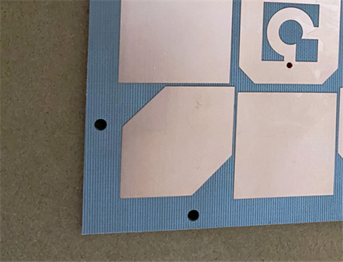
2. Wangling F4BTMS1000 PCB Features
Dk (10 GHz): 10.2 ± tight tolerance, excellent batch consistency
Df (10/20 GHz): 0.0020 / 0.0023 – ultra-low signal loss
CTE (X/Y/Z): 16 / 18 / 32 ppm/°C (-55°C to 288°C)
Thermal Coefficient of Dk: -320 ppm/°C (-55°C to 150°C) – stable phase/frequency
Thermal Conductivity: 0.81 W/mK – efficient heat dissipation
Moisture Absorption: 0.03% – stable in high humidity
Board Thickness: 0.4 mm
Cu Weight (outer layers): 1 oz (1.4 mils)
Surface Finish: OSP
Min Trace/Space: 5/6 mils
Min Hole Size: 0.2 mm
100% Electrical Testing (pre-shipment)
Radiation Resistance: stable after high-dose irradiation
Ultra-Low Outgassing: meets aerospace vacuum requirements
Superior Dimensional Stability – for high-density precision circuits
3. Wangling F4BTMS1000 PCB Benefits
Aerospace-grade reliability – radiation resistant, low outgassing
Ultra-low dielectric loss – minimizes RF signal attenuation
Stable phase/frequency – up to 40 GHz, -55°C to 288°C
High thermal conductivity – improves high-power system reliability
Low CTE – excellent thermal stability and PTH reliability
Superior dimensional stability – consistent circuit geometry
Excellent machinability – supports fine-line, dense vias, multilayer
High cost-performance – domestic alternative to imported aerospace laminates
Mature mass production – consistent quality and global supply
4. PCB Construction Details
Base material |
F4BTMS1000 |
Layer count |
2 layers |
Board dimensions |
79.6mm x 45 mm=1PCS, +/- 0.15mm |
Minimum Trace/Space |
5/6 mils |
Minimum Hole Size |
0.2mm |
Blind vias |
No |
Finished board thickness |
0.4mm |
Finished Cu weight |
1oz (1.4 mils) outer layers |
Via plating thickness |
20 μm |
Surface finish |
OSP |
Top Silkscreen |
No |
Bottom Silkscreen |
No |
Top Solder Mask |
No |
Bottom Solder Mask |
No |
Electrical test |
100% Electrical test used prior to shipment |
5. PCB Stackup
2-layer rigid PCBCopper_layer_1 - 35μm (1oz)Wangling F4BTMS1000 Core - 0.254 mm (10mil)Copper_layer_2 - 35μm (1oz)
6. PCB Statistics
·Components: 42·Total Pads: 78·Thru Hole Pads: 41·Top SMT Pads: 37·Bottom SMT Pads: 0·Vias: 36·Nets: 2
7. Type Of Artwork Supplied
Gerber RS-274-X
8. Quality Standard
IPC-Class-2
9. Availability
Worldwide
10. Wangling F4BTMS1000 PCB Applications
- Aerospace equipment, space and cabin equipment
- Microwave, RF
- Radar, military radar
- Feed networks
- Phase-sensitive antennas, phased array antennas
- Satellite communications, and more.
11. Wangling F4BTMS1000 CCL Base Material Knowledge
11.1 Material Overview
Wangling F4BTMS1000 is a professional-grade aerospace copper clad laminate (CCL) specially developed by Wangling for high performance RF, microwave, radar and extreme environment electronic applications. It is the core grade of the F4BTMS series, an upgraded iteration of the F4BTM series with groundbreaking technological breakthroughs in material formulation and manufacturing processes. It adopts an innovative composite structure of high-purity PTFE resin, uniformly distributed special nano-ceramics, and ultra-thin ultra-fine woven fiberglass cloth reinforcement, delivering exceptional electrical performance, mechanical stability, and environmental adaptability.
By incorporating a small amount of ultra-thin ultra-fine glass fiber cloth and a large amount of uniformly distributed special nano-ceramics mixed with PTFE resin, the F4BTMS1000 minimizes the negative glass fiber weave effect on electromagnetic wave propagation. This innovative design reduces dielectric loss, enhances dimensional stability, decreases the X/Y/Z anisotropy of the material, extends the usable frequency range up to 40GHz, improves electrical strength, and enhances thermal conductivity. Additionally, the material exhibits an excellent low thermal expansion coefficient and stable dielectric temperature characteristics across a wide temperature range of -55°C to 288°C.
The F4BTMS series comes standard with RTF low-roughness copper foil, which reduces conductor loss at high frequencies while providing excellent peel strength. It can be paired with either copper or aluminum bases for different thermal management requirements, and the F4BTMS294 grade can be paired with embedded 50Ω resistive copper foil to form resistive film laminates. The F4BTMS1000 laminate is fully compatible with standard PTFE PCB processing technology, with excellent mechanical and physical properties that make it suitable for multilayer, high-multilayer, and backplane processing. It also delivers outstanding machinability for high-density fine-line circuits and dense via hole fabrication, making it the ideal substrate for modern high frequency electronic designs.
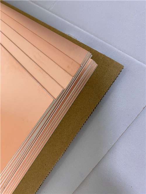
11.2 F4BTMS1000 CCL Core Benefits
·Tight dielectric constant tolerance and excellent batch-to-batch consistency, ensuring stable impedance matching and consistent circuit performance across mass production batches·Ultra-low dielectric loss for high efficiency RF signal transmission and minimal signal attenuation at high microwave frequencies·Wide operating frequency range, maintaining stable dielectric constant and low loss values at frequencies up to 40GHz, fully meeting the requirements of phase-sensitive applications·Excellent temperature stability, with dielectric constant and dissipation factor maintaining excellent frequency and phase stability across -55°C to 150°C·Superior radiation resistance, maintaining stable dielectric and physical properties after high-dose irradiation, making it ideal for aerospace and space applications·Ultra-low outgassing performance, tested in accordance with standard methods for material volatilization under vacuum conditions, fully complying with aerospace vacuum outgassing requirements·Low X/Y/Z-axis thermal expansion coefficient, ensuring excellent dimensional thermal stability and plated through hole reliability even under extreme thermal cycling conditions·High thermal conductivity of 0.81 W/mK, effectively dissipating heat generated by high-power components and adapting to high-power RF and microwave application scenarios·Excellent dimensional stability, maintaining consistent circuit geometry and electrical performance across varying temperature and environmental conditions·Low moisture absorption of 0.03%, ensuring stable electrical performance in high-humidity operating environments·Mature mass production capability ensures stable product quality and consistent supply for large-scale commercial projects·Excellent cost-performance ratio as a high-performance domestic alternative to imported aerospace-grade high frequency laminates
11.3 F4BTMS1000 CCL Typical Applications
·Aerospace & Aviation Equipment, Space and Cabin On-Board Electronics·Microwave, RF and High Power Amplifier Circuits·Radar Systems, Military Radar and Phased Array Radar·Antenna Feed Networks and Phase-Sensitive Antennas·Phased Array Antennas for 5G/6G Base Stations·Satellite Communication On-Board Electronic Systems·Avionics and Aircraft Collision Avoidance Systems·Test and Measurement Instrumentation RF Circuits·Industrial Microwave Heating and High Power RF Equipment·Automotive Radar and Advanced Driver Assistance System (ADAS) RF Circuits
12. DataSheet
Parameter Name |
Parameter Value |
Base material |
F4BTMS1000 |
Layer count |
2 layers |
Board dimensions |
79.6mm x 45 mm=1PCS, +/- 0.15mm |
Minimum Trace/Space |
5/6 mils |
Minimum Hole Size |
0.2mm |
Blind vias |
No |
Finished board thickness |
0.4mm |
Finished Cu weight |
1oz (1.4 mils) outer layers |
Via plating thickness |
20 μm |
Surface finish |
OSP |
Top Silkscreen |
No |
Bottom Silkscreen |
No |
Top Solder Mask |
No |
Bottom Solder Mask |
No |
Electrical test |
100% Electrical test used prior to shipment |
13. Summary
Wangling F4BTMS1000 2-Layer 0.4mm High Frequency PCB is an aerospace-grade, high-reliability rigid circuit board built with advanced ceramic filled PTFE composite substrate from Wangling. With its precise dielectric performance, ultra-low loss high frequency characteristics, exceptional phase and temperature stability, aerospace-grade radiation resistance and low outgassing performance, high thermal conductivity, and superior mechanical reliability, this Wangling F4BTMS1000 2-Layer PCB fully adapts to aerospace, satellite communication, radar, phased array antenna, and high-power RF microwave electronic projects. It supports global supply chain coverage and fully meets IPC Class 2 quality standard requirements for mass production.
Tags:Wangling F4BTMS1000 PCB, 2 Layer F4BTMS1000 High Frequency PCB, 0.4mm Thin Rigid RF PCB, OSP Surface Finish PCB, IPC Class 2 High Frequency PCB, Ceramic Filled PTFE CCL, Wangling F4BTMS1000 Copper Clad Laminate,, Wangling F4BTMS Series PCB