

 Home
-
Newly shipped PCBs
-
F4BME217 2-Layer Copper Clad Laminate PCB Wangling 1mm Custom DK PTFE Laminate for RF Microwave Use
Home
-
Newly shipped PCBs
-
F4BME217 2-Layer Copper Clad Laminate PCB Wangling 1mm Custom DK PTFE Laminate for RF Microwave Use
F4BME217 2-Layer Copper Clad Laminate PCB Wangling 1mm Custom DK PTFE Laminate for RF Microwave Use
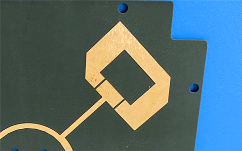
Printed Circuit Boards are custom-made products; the images and specifications provided are for reference only.
1. Wangling F4BME217 PCB Introduction
Wangling F4BME217 is a high-performance PTFE composite copper clad laminate developed by Wangling, a leading domestic manufacturer of high frequency electronic materials, engineered for demanding RF, microwave and millimeter wave circuit applications. F4BME217 high- frequency laminate is precision-formulated from woven fiberglass cloth, polytetrafluoroethylene (PTFE) resin and PTFE film, manufactured through scientific formulation and strict process pressing to deliver superior and consistent electrical properties.
As a next-generation high frequency laminate, Wangling F4BME217 significantly outperforms its predecessor F4B220, featuring lower dielectric loss, higher insulation resistance, and enhanced long-term performance stability. It serves as a reliable, high-performance domestic substitute for comparable imported high frequency laminates, providing a cost-effective solution for commercial and industrial high frequency circuit mass production. This 2-layer 1.3mm F4BME217 PCB is built with Wangling’s proprietary F4BME217 core material, clad with Reverse-Treated Foil (RTF) copper to deliver superior low-PIM performance, enable more precise etching for fine-line circuits, and reduce conductor loss, making it ideal for high-precision RF and microwave circuit designs.
Wangling’s F4B series laminates include three core grades: F4BM, F4BME and F4BME217, all sharing the same high-performance PTFE-fiberglass composite dielectric layer, differentiated by their matched copper foil configurations and performance tuning. F4BM is paired with standard ED copper foil, suitable for applications without strict PIM index requirements; F4BME and F4BME217 are paired with reverse-treated RTF copper foil, delivering excellent PIM performance, more precise circuit line control, and lower conductor loss for high-precision RF designs.
2. Wangling F4BME217 PCB Features
- Customizable Dielectric Constant (DK): 2.17~3.0 optional, with custom DK values available on demand
- Ultra-low dielectric loss for high efficiency RF signal transmission
- Clad with Reverse-Treated Foil (RTF) copper for excellent low-PIM performance
- Precise line width control for high-density fine-line circuit fabrication
- Finished Board Thickness: 1.3mm
- Finished Cu Weight: 1oz (1.4 mils) outer layers
- Bare Copper Surface Finish
- Minimum Trace/Space: 5/6 mils
- Minimum Hole Size: 0.25mm
- 100% Pre-Shipment Electrical Testing
- Radiation resistance and low outgassing performance for aerospace applications
- Diverse size options for cost-effective mass production
3. Wangling F4BME217 PCB Benefits
- Customizable DK value enables perfect matching of circuit impedance requirements for different RF and microwave designs
- Ultra-low dielectric loss minimizes signal attenuation and improves overall circuit transmission efficiency
- Excellent low-PIM performance meets the strict requirements of high-precision communication and radar systems
- Superior dimensional stability ensures consistent circuit performance across varying temperature and environmental conditions
- Low thermal expansion coefficient and temperature drift deliver stable electrical performance in extreme operating environments
- High cost-performance ratio supports large-scale commercial mass production of high frequency electronic devices
- Radiation resistance and low outgassing characteristics make it suitable for aerospace and satellite communication applications
- Fully compatible with standard PCB processing workflows for easy fabrication and mass production
4. PCB Construction Details
Item |
Specification |
Board Dimensions |
102 mm x 83 mm, 1PCS, +/- 0.15mm |
Minimum Trace/Space |
5/6 mils |
Minimum Hole Size |
0.25mm |
Blind Vias |
No Blind vias |
Finished Board Thickness |
1.3mm |
Finished Cu Weight |
1oz (1.4 mils) outer layers |
Via Plating Thickness |
20 μm |
Surface Finish |
Bare copper |
Top Silkscreen |
No |
Bottom Silkscreen |
No |
Top Solder Mask |
No |
Bottom Solder Mask |
No |
Pre-Shipment Inspection |
100% Electrical test prior to shipment |
5. PCB Stackup
2-layer rigid PCBCopper_layer_1 - 35μm (1oz)Wangling F4BME217 Core - 1.0 mm (39.37mil)Copper_layer_2 - 35μm (1oz)
6. PCB Statistics
- Components: 15
- Total Pads: 42
- Thru Hole Pads: 17
- Top SMT Pads: 25
- Bottom SMT Pads: 0
- Vias: 28
- Nets: 7
7. Type Of Artwork Supplied
Gerber RS-274-X
8. Quality Standard
IPC-Class-2
9. Availability
Worldwide
10. Wangling F4BME217 PCB Applications
- Microwave, RF and Radar System Circuits
- Phase Shifters and High Precision Passive RF Components
- Power Dividers, Directional Couplers and Power Combiners
- Antenna Feed Networks and Phased Array Antennas
- Satellite Communication On-Board Electronics
- 5G/6G Base Station Antenna and RF Front-End Circuits
- Aerospace and Defense High Frequency Electronic Systems
- Test and Measurement Instrumentation RF Circuits
11. Wangling F4BME217 CCL Base Material Knowledge
11.1 Material Overview
Wangling F4BME217 is a professional-grade copper clad laminate (CCL) specially developed by Wangling for high performance RF, microwave and millimeter wave electronic applications. It adopts an advanced composite structure of woven fiberglass cloth reinforced PTFE resin, combined with PTFE film, manufactured through scientific formulation optimization and strict high-temperature pressing process. The electrical and mechanical properties of F4BME217 are precisely tuned by adjusting the ratio of PTFE resin to fiberglass cloth within the composite, enabling controlled dielectric constant values while maintaining low loss characteristics and enhanced dimensional stability.
A higher dielectric constant is achieved by increasing the fiberglass content in the composite, which simultaneously improves dimensional stability, lowers the thermal expansion coefficient, and reduces temperature drift of electrical properties. This design involves a balanced trade-off, as a higher fiberglass ratio may result in a marginal increase in dielectric loss, allowing engineers to select the optimal material grade for a perfect balance of electrical performance, mechanical robustness, and processing requirements. With a customizable DK range of 2.17 to 3.0, Wangling F4BME217 can be tailored to meet the specific impedance and performance requirements of different high frequency circuit designs.
As a domestic high-performance high frequency laminate, Wangling F4BME217 delivers comparable or superior performance to imported equivalent products, with the advantages of shorter lead times, flexible customization options, and excellent cost-performance ratio for mass production. It is fully compatible with conventional PTFE PCB processing workflows, supporting standard shearing, drilling, milling, etching and plating procedures, making it easy to integrate into existing PCB manufacturing processes.
 F4BME217.jpg)
11.2 F4BME217 CCL Core Benefits
- Customizable dielectric constant (DK 2.17~3.0) to perfectly match different circuit design requirements
- Ultra-low dielectric loss for high efficiency RF signal transmission and minimal signal attenuation
- Reverse-Treated Foil (RTF) copper cladding delivers excellent low-PIM performance for high precision communication systems
- Precise tuning of PTFE-fiberglass ratio balances electrical performance, mechanical strength and processing adaptability
- High fiberglass content grades deliver superior dimensional stability, low thermal expansion coefficient and minimal temperature drift
- Radiation resistance and low outgassing characteristics meet the strict requirements of aerospace and satellite applications
- Diverse standard size options and custom cutting services reduce material waste and lower overall production costs
- Mature mass production capability ensures stable product quality and consistent supply for large-scale commercial projects
- Excellent cost-performance ratio as a high-performance domestic alternative to imported high frequency laminates
11.3 F4BME217 CCL Typical Applications
- Microwave, RF and Radar System Circuits
- Phase Shifters and High Precision Passive RF Components
- Power Dividers, Directional Couplers and Power Combiners
- Antenna Feed Networks and Phased Array Antennas
- Satellite Communication On-Board Electronics
- 5G/6G Base Station Antenna and RF Front-End Circuits
- Aerospace and Defense High Frequency Electronic Systems
- Test and Measurement Instrumentation RF Circuits
- Industrial Microwave Heating and Power Amplifier Circuits
- Automotive Radar and Advanced Driver Assistance System (ADAS) RF Circuits
12. DataSheet
Parameter |
Test Condition |
Unit |
Specification |
Notes |
Electrical Properties |
|
|
|
|
Dielectric Constant (Typical Value) |
10GHz |
- |
2.17 |
|
Dielectric Constant Tolerance |
- |
- |
±0.04 |
|
Dissipation Factor (Typical Value) |
10GHz |
- |
0.001 |
|
Dissipation Factor (Typical Value) |
20GHz |
- |
0.0014 |
|
Thermal Coefficient of Dielectric Constant |
-55℃~150℃ |
ppm/℃ |
-150 |
|
Volume Resistivity |
Normal Condition |
MΩ·cm |
≥6×10⁶ |
|
Surface Resistivity |
Normal Condition |
MΩ |
≥1×10⁶ |
|
Dielectric Strength (Z-direction) |
5KW, 500V/s |
kV/mm |
>23 |
|
Breakdown Voltage (XY-direction) |
5KW, 500V/s |
kV |
>30 |
|
Mechanical Properties |
|
|
|
|
Copper Peel Strength |
1 OZ F4BM |
N/mm |
>1.8 |
|
Copper Peel Strength |
1 OZ F4BME |
N/mm |
>1.6 |
|
Thermal Properties |
|
|
|
|
Coefficient of Thermal Expansion (CTE) - XY Direction |
-55℃~288℃ |
ppm/℃ |
25/34 |
|
Coefficient of Thermal Expansion (CTE) - Z Direction |
-55℃~288℃ |
ppm/℃ |
240 |
|
Thermal Stress |
260℃, 10s, 3 Cycles |
- |
No Delamination |
|
Continuous Operating Temperature |
High & Low Temperature Chamber |
℃ |
-55~+260 |
|
Thermal Conductivity |
Z-direction |
W/(m·K) |
0.24 |
|
Decomposition Temperature (Td) |
2hrs @ 105℃, 5% Weight Loss |
℃ |
500 |
|
Physical Properties |
|
|
|
|
Moisture Absorption |
20±2℃, 24 Hours |
% |
≤0.08 |
|
Density |
Room Temperature |
g/cm³ |
2.17 |
|
Specific Heat Capacity |
2 Hours at 105℃ |
J/g·K |
0.93 |
|
Flammability |
- |
UL-94 |
V-0 |
|
Comparative Tracking Index |
- |
V/PLC |
600V/PLC 0 |
|
Other Specifications |
|
|
|
|
Passive Intermodulation (PIM) Value |
F4BME Only |
dBc |
≤-159 |
|
Material Composition |
- |
- |
PTFE, Fiberglass Cloth |
F4BM is matched with ED copper foil; F4BME is matched with reversed RTF copper foil |
Pre-Shipment Inspection |
- |
- |
100% Electrical Test Prior to Shipment |
|
13. Summary
Wangling F4BME217 2-Layer 1.3mm High Frequency PCB is a cost-effective, high-performance rigid circuit board built with advanced customizable DK PTFE-fiberglass composite substrate from Wangling. With its tunable dielectric constant, ultra-low loss high frequency performance, excellent low-PIM characteristics, superior dimensional stability and reliable mechanical performance, this Wangling F4BME217 2-Layer PCB fully adapts to microwave, RF, radar, satellite communication, 5G base station and aerospace high frequency electronic projects. It supports global supply chain coverage and fully meets IPC Class 2 quality standard requirements for mass production.
Tags:Wangling F4BME217 PCB, 2 Layer F4BME217 High Frequency PCB, 1.3mm Rigid RF PCB, Bare Copper Surface Finish PCB, IPC Class 2 High Frequency PCB, PTFE Fiberglass CCL, Wangling F4BME217 Copper Clad Laminate, Customizable DK RF PCB, Low PIM Microwave PCB, Radar System PCB, Satellite Communication PCB, 5G Base Station Antenna PCB, Domestic High Frequency Laminate, Wangling F4B Series PCB