

 Home
-
Newly shipped PCBs
-
Dual Layer PCB built on 10mil F4BTMS430 Substrate High-Reliability Aerospace and RF laminate with Immersion Gold
Home
-
Newly shipped PCBs
-
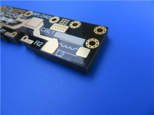
Dual Layer PCB built on 10mil F4BTMS430 Substrate High-Reliability Aerospace and RF laminate with Immersion Gold
Dual Layer PCB built on 10mil F4BTMS430 Substrate High-Reliability Aerospace and RF laminate with Immersion Gold
Printed Circuit Boards are custom-made products; the images and specifications provided are for reference only.
1. F4BTMS430 PCB Introduction
Wangling F4BTMS430 circuit board is constructed using F4BTMS430 laminates, the advanced upgraded version of the F4BTM series. F4BTMS430 premium PCB board achieves remarkable technological advancements in material formulation and manufacturing processes, integrating a high concentration of ceramic components and reinforced with ultra-thin, ultra-fine glass fiber cloth. Such innovations significantly enhance overall material performance while expanding the range of available dielectric constants, making it a high-reliability solution tailored for aerospace applications and a viable alternative to comparable foreign products.
F4BTMS430 PCB substrate consists of a precise blend of ultra-thin, ultra-fine glass fiber cloth, uniformly dispersed special nano-ceramics, and polytetrafluoroethylene (PTFE) resin. F4BTMS laminate's unique composition minimizes the adverse impacts of glass fiber on electromagnetic wave propagation, thereby reducing dielectric loss, boosting dimensional stability, and lowering the X/Y/Z anisotropy of the material. F4BTMS430 high-frequency laminates further extends the usable frequency range, improves electrical strength, and enhances thermal conductivity, while maintaining excellent low thermal expansion coefficient and stable dielectric temperature characteristics. As a standard configuration, Wangling F4BTMS430 PCB adopts RTF low-roughness copper foil, which effectively reduces conductor loss and ensures superior peel strength. It is compatible with both copper and aluminum substrates, offering versatile integration options for diverse high-performance applications.
2. Key Features of Wangling F4BTMS430 PCB
- Dielectric Constant (Dk): 4.3 at 10GHz
- Dissipation Factor: 0.0019 at 10GHz; 0.0024 at 20GHz
- Coefficient of Thermal Expansion (CTE): X-axis 13 ppm/°C, Y-axis 12 ppm/°C, Z-axis 47 ppm/°C (Temperature range: -55°C to 288°C)
- Low Thermal Coefficient of Dk: -60 ppm/°C (Temperature range: -55°C to 150°C)
- High Thermal Conductivity: 0.63 W/mk
- Low Moisture Absorption: 0.08%
- Flammability Rating: UL-94V0
3. Core Benefits of Wangling F4BTMS430 PCB
- Enhanced Signal Integrity: Minimized dielectric loss and reduced conductor loss (via RTF low-roughness copper foil) ensure stable signal transmission in high-frequency RF and microwave applications.
- Superior Dimensional Stability: Low X/Y/Z anisotropy and excellent CTE performance prevent board warpage and component damage under extreme temperature fluctuations, enhancing long-term reliability.
- Broad Application Versatility: Compatible with copper and aluminum substrates, coupled with a wide usable frequency range, making it suitable for diverse critical applications including aerospace and military systems.
- High Environmental Resistance: Low moisture absorption (0.08%) and UL-94V0 flammability rating meet strict safety and environmental requirements for harsh operating environments.
- Cost-Effective Alternative: High-performance characteristics enable it to replace foreign counterparts, providing a reliable and cost-efficient solution for high-reliability electronic systems.
4. PCB Construction Specifications
- Base Material: F4BTMS430
- Layer Count: 2 Layers
- Board Dimensions: 78.63mm x 96.55mm per piece, Tolerance: +/- 0.15mm
- Minimum Trace/Space: 6/6 mils
- Minimum Hole Size: 0.3mm
- Blind Vias: Not Available
- Finished Board Thickness: 0.3mm
- Finished Copper Weight: 1oz (1.4 mils) for Outer Layers
- Via Plating Thickness: 20 μm
- Surface Finish: Immersion Gold (ENIG)
- Top Silkscreen: White
- Bottom Silkscreen: No
- Top Solder Mask: Black
- Bottom Solder Mask: No
- Quality Control: 100% Electrical Test Conducted Prior to Shipment
5. PCB Stackup Configuration
2-Layer Rigid PCB with the Following Stackup:
- Copper Layer 1: 35 μm
- F4BTMS430 Core: 0.254mm (10mil)
- Copper Layer 2: 35 μm
6. PCB Technical Statistics
- Total Components: 15
- Total Pads: 62
- Thru Hole Pads: 30
- Top SMT Pads: 32
- Bottom SMT Pads: 0
- Vias: 25
- Nets: 2
7. Artwork Specification
Type of Artwork Supplied: Gerber RS-274-X
8. Quality Standard
Complies with IPC-Class-2
9. Global Availability
Available for Worldwide Shipping
10. Typical Application Fields
- Aerospace Equipment, Space and Cabin Equipment
- Microwave and RF Devices
- Radar Systems, Military Radar
- Feed Networks
- Phase-Sensitive Antennas, Phased Array Antennas
- Satellite Communication Systems, and More
11. Product Summary
F4BTMS430 Double Sided PCB is a high-performance rigid substrate engineered for critical high-frequency and high-reliability applications. Leveraging the advanced F4BTMS430 laminate technology, this PCB delivers exceptional dielectric performance, low loss, superior dimensional stability, and excellent thermal conductivity. Compliant with IPC-Class-2 quality standards and featuring Immersion Gold (ENIG) surface finish, it meets the rigorous requirements of aerospace, military, and satellite communication industries. With its ability to replace foreign counterparts and worldwide availability, Wangling F4BTMS430 laminate PCB offers a reliable, versatile, and cost-effective solution for demanding electronic systems.
Founded in 2003, Shenzhen Bicheng Electronics Technology Co., Ltd is an established high frequency PCB supplier and exporter in Shenzhen, China, serving customers worldwide.
We are devoted to delivering high-frequency PCB products and solutions of the highest quality, along with customized service. Get in touch with us to start your project !
Visit https://www.bicheng-enterprise.com to learn more.