

 Home
-
Newly shipped PCBs
-
Rogers RO4350B and S1000-2M Hybrid PCB 6-Layer 4mil High Tg FR-4 PCB for RF and Microwave Applications
Home
-
Newly shipped PCBs
-
Rogers RO4350B and S1000-2M Hybrid PCB 6-Layer 4mil High Tg FR-4 PCB for RF and Microwave Applications
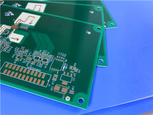
Rogers RO4350B and S1000-2M Hybrid PCB 6-Layer 4mil High Tg FR-4 PCB for RF and Microwave Applications
Printed Circuit Boards are custom-made products; the images and specifications provided are for reference only.
1.Rogers RO4350B Hybrid PCB Introduction
Rogers RO4350B and S1000-2M 6-Layer 1.3mm High-Frequency PCB features base materials including Rogers RO4350B laminate , a proprietary woven glass-reinforced hydrocarbon/ceramic composite. This material delivers electrical performance comparable to PTFE/woven glass while maintaining the manufacturability of epoxy/glass laminates.
Rogers RO4350B PCB offers tight dielectric constant (Dk) control and low loss, compatible with standard epoxy/glass processing methods. Cost-effective compared to conventional microwave laminates, it eliminates the need for special through-hole treatments or handling procedures required by PTFE-based materials. UL 94 V-0 rated, it is ideal for active devices and high-power RF designs. Its thermal coefficient of expansion (CTE) closely matches copper, ensuring excellent dimensional stability for mixed-dielectric multi-layer constructions. With a low Z-axis CTE, Rogers RO4350B PCB guarantees reliable plated through-hole quality even under severe thermal shock. Boasting a Tg of >280°C (536°F), its expansion characteristics remain stable across all circuit processing temperatures.
2.PCB Construction details:
Base material: RO4350B and High Tg FR-4 (S1000-2M)
Layer count: 6-layer
Board dimensions: 30.55mm x 37.7mm=1PCS, +/- 0.15mm
Minimum Trace/Space: 4/4 mils
Minimum Hole Size: 0.25mm
Blind vias L1-L2
Finished board thickness: 1.3mm
Finished Cu weight: 1oz (1.4 mils) inner/outer layers
Via plating thickness: 20 μm
Surface finish: Electroless Nickle Electroless Palladium Immersion Gold (ENEPIG)
Top Silkscreen: White
Bottom Silkscreen: White
Top Solder Mask: No
Bottom Solder Mask: Green
100% Electrical test used prior to shipment
3.PCB Stackup: 6-layer rigid PCB
Copper_layer_1 - 35 μm
RO4350B - 0.102mm (4mil)
Copper_layer_2 - 35 μm
Prepreg - 1080 RC63% +7628 (43%) -0.254mm (10mil)
Copper_layer_3 - 35 μm
S1000-2M - 0.254 mm (10mil)
Copper_layer_4 - 35 μm
Prepreg - 1080 RC63% +7628 (43%) -0.254mm (10mil)
Copper_layer_5 - 35 μm
S1000-2M - 0.254 mm (10mil)
Copper_layer_6 - 35 μm
4.PCB Statistics:
Components: 8
Total Pads: 39
Thru Hole Pads: 21
Top SMT Pads: 12
Bottom SMT Pads: 6
Vias: 23
Nets: 10
5. 1 Features (S1000-2M)
Lower Z-Axis CTE for improved throughhole reliability
Excellent Mechanical Processability and Thermal Resistance
Leadfree Compatible
Tg180℃ (DSC), UV Blocking/AOI compatible
High heat resistance
Excellent Anti-CAF performance
Low water absorption
5.2 Features (RO4350B)
Dielectric Constant of DK 3.48 +/-0.05 at 10GHz/23°C
Dissipation Factor of 0.0037 at 10GHz/23°C
Thermal Conductivity 0.69 W/m/°K
X axis CTE of 10 ppm/°C, Y CTE of 12 ppm/°C, Z CTE of 32 ppm/°C
High Tg value of >280 °C
Low water absorption of 0.06%
6.Type of artwork supplied: Gerber RS-274-X
7.Accepted standard: IPC-Class-2
8.Availability: worldwide
9.Some Typical Applications:
Commercial Airline Broadband Antennas
Microstrip and Stripline Circuits
Millimeter Wave Applications
Radar Systems
Guidance Systems
Point to Point Digital Radio Antennas