

 Home
-
Newly shipped PCBs
-
10mil Rogers RO4350B and High Tg FR-4 Circuit Board 4-Layer Hybrid PCB with Impedance Controlled for RF Applications
Home
-
Newly shipped PCBs
-
10mil Rogers RO4350B and High Tg FR-4 Circuit Board 4-Layer Hybrid PCB with Impedance Controlled for RF Applications
10mil Rogers RO4350B and High Tg FR-4 Circuit Board 4-Layer Hybrid PCB with Impedance Controlled for RF Applications
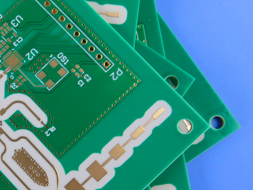
Printed Circuit Boards are custom-made products; the images and specifications provided are for reference only.
1. Product Spotlight: High-Frequency Hybrid Dielectric PCB
This technical overview presents a sophisticated 4-layer rigid printed circuit board engineered for high-frequency and RF applications. This hybrid board utilizes a hybrid construction combining Rogers RO4350B hydrocarbon ceramic laminate with high Tg FR-4 materials, delivering exceptional electrical performance while maintaining mechanical stability and cost-effectiveness. The inclusion of blind vias and precise 50-ohm impedance control makes this board ideally suited for demanding microwave and millimeter wave circuits.
The complete specifications of this board are outlined in the table below.
Specification |
Details |
Base Material |
RO4350B + High Tg 170°C FR-4 Hybrid |
Layer Count |
4 Layers |
Board Dimensions |
35 mm x 25 mm per unit, +/- 0.15 mm |
Minimum Trace/Space |
4 mil / 4 mil |
Minimum Hole Size |
0.30 mm |
Via Structure |
Blind Vias L3-L4 |
Finished Board Thickness |
1.55 mm |
Copper Weight |
1 oz (35 μm) Inner and Outer Layers |
Via Plating Thickness |
20 μm |
Surface Finish |
Electroless Nickel Immersion Gold (ENIG) |
Top Silkscreen |
White |
Bottom Silkscreen |
Green |
Top Solder Mask |
Green |
Bottom Solder Mask |
Green |
Impedance Control |
50 ohm, Top Side, 5/8 mil Differential Pairs |
Electrical Testing |
100% Electrical Test Prior to Shipment |
Artwork Format |
Gerber RS-274-X |
Manufacturing Standard |
IPC-Class-2 |
Availability |
Worldwide |
2. Understanding RO4350B High-Frequency Laminate Material
2.1 Introduction to RO4350B
RO4350B is a proprietary woven glass reinforced hydrocarbon and ceramic laminate material manufactured by Rogers Corporation. This material bridges the performance gap between traditional PTFE-based microwave laminates and standard epoxy-glass materials. It delivers electrical performance approaching that of PTFE/woven glass while offering the manufacturability and ease of processing associated with epoxy/glass materials.
The key advantages of RO4350B include its compatibility with standard epoxy/glass processing methods, eliminating the need for special through-hole treatments or handling procedures required by PTFE-based materials. At a fraction of the cost of conventional microwave laminates, RO4350B provides an economical solution for high-frequency circuit designs while maintaining UL 94 V-0 rating suitable for active devices and high power RF applications.
The thermal coefficient of expansion characteristics of RO4350B closely match that of copper, providing excellent dimensional stability essential for mixed dielectric multi-layer board constructions. The low Z-axis CTE ensures reliable plated through-hole quality even under severe thermal shock conditions, while the Tg exceeding 280°C maintains stable expansion characteristics across the entire range of circuit processing temperatures.
2.2 Key Features of RO4350B Material
The RO4350B material offers the following performance characteristics:
Dielectric Constant of 3.48 +/- 0.05 measured at 10GHz and 23°C, providing consistent and predictable impedance control
Dissipation Factor of 0.0037 at 10GHz and 23°C, ensuring low signal loss at high frequencies
Thermal Conductivity of 0.69 W/m/°K, facilitating efficient heat dissipation from active components
Coefficient of Thermal Expansion of 10 ppm/°C in X axis, 12 ppm/°C in Y axis, and 32 ppm/°C in Z axis for reliable thermal performance
Glass Transition Temperature exceeding 280°C, maintaining structural integrity during assembly and operation
Low Water Absorption of 0.06%, preserving electrical properties in humid environments
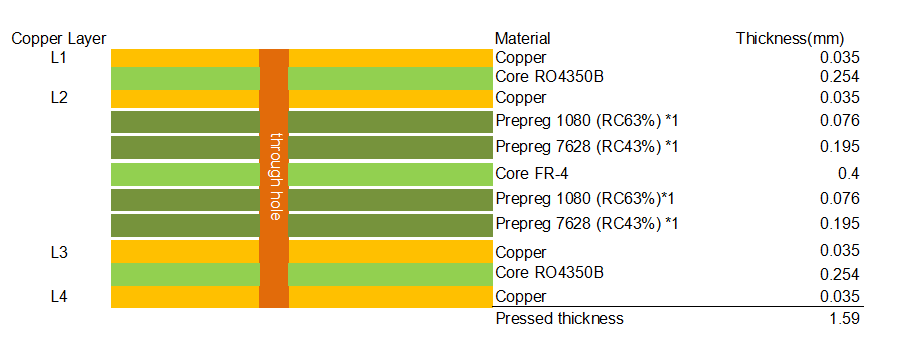
3. PCB Stackup Construction and Layer Configuration
3.1 Detailed Layer Stackup
This 4-layer board employs a symmetric hybrid stackup designed to optimize signal integrity and mechanical stability. The construction begins with Layer 1 as the top signal layer with 35 μm copper, directly bonded to 0.254 mm RO4350B dielectric material. Layer 2 serves as an internal signal or ground plane with 35 μm copper.
The core construction continues with a prepreg combination of 1080 RC63% and 7628 with 43% resin content, totaling 0.254 mm thickness, bonding to the 0.4 mm High Tg 170°C FR-4 core material. Another identical prepreg layer of 1080 RC63% and 7628 at 0.254 mm thickness follows before reaching Layer 3 with 35 μm copper.
Layer 3 is bonded to the final 0.254 mm RO4350B dielectric layer, with Layer 4 serving as the bottom signal or ground plane with 35 μm copper. This symmetrical construction ensures balanced thermal and mechanical properties while providing excellent high-frequency performance through the RO4350B outer layers.
3.2 Blind Via Structure L3-L4
The board incorporates blind vias connecting Layer 3 to Layer 4, enabling high-density interconnect routing without compromising signal integrity. These blind vias are plated with 20 μm copper thickness, ensuring reliable electrical connections while maintaining controlled impedance characteristics. The blind via construction reduces signal path length and minimizes parasitic inductance compared to through-hole alternatives, particularly beneficial for high-frequency applications.
4. PCB Design Statistics and Assembly Considerations
4.1 Component and Pad Configuration
The board design accommodates 17 total components distributed across both sides, with 45 total pads providing interconnection points. The pad configuration includes 21 through-hole pads for traditional leaded components, 16 surface mount pads on the top side, and 8 surface mount pads on the bottom side. This balanced distribution allows for flexible component placement and optimized circuit layout.
4.2 Via and Network Configuration
Nine vias facilitate interlayer connections throughout the board, supporting 10 distinct electrical nets. This via count, combined with the blind via structure, provides ample routing flexibility while maintaining signal integrity for high-frequency paths.
5. Impedance Control and Signal Integrity
5.1 50 Ohm Controlled Impedance Design
The top side features precisely controlled 50 ohm impedance traces with 5/8 mil differential pair spacing, essential for matching transmission line characteristics in RF and microwave circuits. This impedance control minimizes signal reflections and ensures maximum power transfer between components, critical for applications operating at frequencies up to millimeter wave ranges.
5.2 Manufacturing Precision
Achieving 4 mil trace and space resolution with 0.30 mm minimum hole size demonstrates the advanced manufacturing capabilities employed for this board. These fine features, combined with precise impedance control, enable high-density RF designs without compromising electrical performance.
6. Quality Assurance and Industry Compliance
6.1 100% Electrical Testing
Every board undergoes comprehensive electrical testing prior to shipment, verifying continuity, isolation, and impedance characteristics. This testing ensures that each board meets the specified performance requirements and functions as designed in the target application.
6.2 IPC-Class-2 Compliance
Manufacturing conforms to IPC-Class-2 standards, the industry benchmark for dedicated service electronic products. This classification ensures extended life and reliable performance while maintaining cost-effectiveness for production volumes. Class 2 compliance guarantees consistent quality suitable for a wide range of commercial and industrial applications.
6.3 Global Availability
These boards are available for worldwide shipment, supported by standard Gerber RS-274-X artwork format compatibility. This ensures seamless integration into existing design and manufacturing workflows regardless of geographic location.
7. Typical Applications
The combination of RO4350B high-frequency performance and FR-4 mechanical stability makes this board suitable for numerous demanding applications:
Commercial Airline Broadband Antennas requiring consistent dielectric properties and environmental stability
Microstrip and Stripline Circuits benefiting from precise impedance control and low signal loss
Millimeter Wave Applications operating at frequencies requiring tight dielectric constant tolerance
Radar Systems demanding reliable performance under varying environmental conditions
Guidance Systems requiring stable electrical characteristics for accurate signal processing
Point to Point Digital Radio Antennas needing low dissipation factor for efficient signal transmission
8. Conclusion
This 4-layer hybrid PCB combining RO4350B and High Tg FR-4 materials delivers exceptional value for high-frequency applications through its precise 50 ohm impedance control on the top side with 5/8 mil differential pairs, enabling reliable signal integrity at microwave frequencies. The blind via structure connecting L3-L4 with 20 μm copper plating facilitates dense routing while maintaining signal quality. The 1.55 mm finished thickness with 1 oz copper on all layers provides mechanical robustness, while the ENIG surface finish ensures excellent solderability and long-term reliability. With 100% electrical testing prior to shipment and IPC-Class-2 compliance, this board meets the rigorous demands of radar systems, broadband antennas, and millimeter wave applications worldwide.
Founded in 2003, Shenzhen Bicheng Electronics Technology Co., Ltd is an established high frequency PCB supplier and exporter in Shenzhen, China, serving customers worldwide.
We are devoted to delivering high-frequency PCB products and solutions of the highest quality, along with customized service. Get in touch with us to start your project !
Visit https://www.bicheng-enterprise.com to learn more.