


 Home
-
Hybrid PCB
-
12-Layer Hybrid PCB with RO4350B and RO3010 Laminates, Nickel-Free Palladium Gold Finish for Microwave & Broadband RF Devices
Home
-
Hybrid PCB
-
12-Layer Hybrid PCB with RO4350B and RO3010 Laminates, Nickel-Free Palladium Gold Finish for Microwave & Broadband RF Devices
12-Layer Hybrid PCB with RO4350B and RO3010 Laminates, Nickel-Free Palladium Gold Finish for Microwave & Broadband RF Devices
Printed Circuit Boards are custom-made products; the images and specifications provided are for reference only.
1. Product Overview
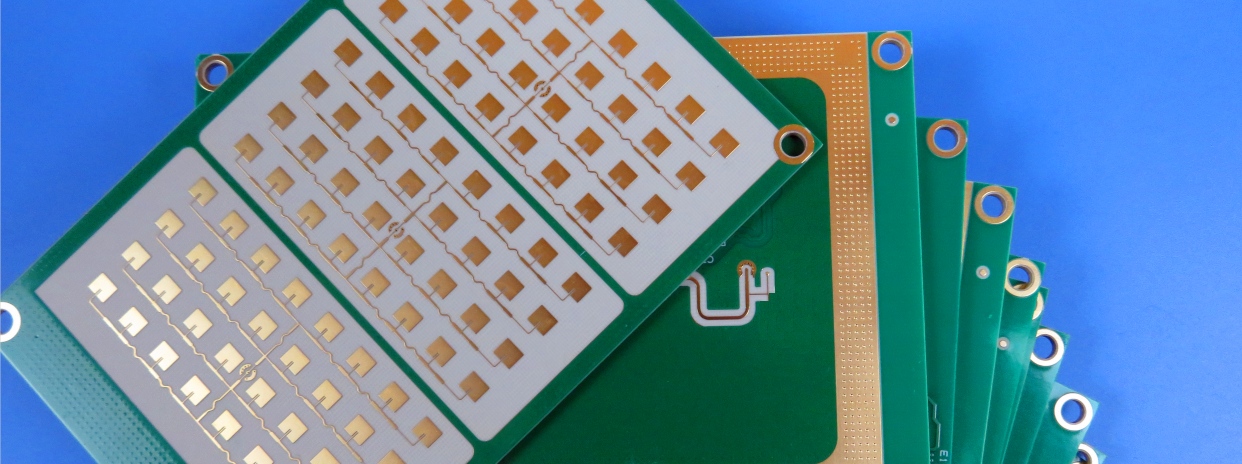
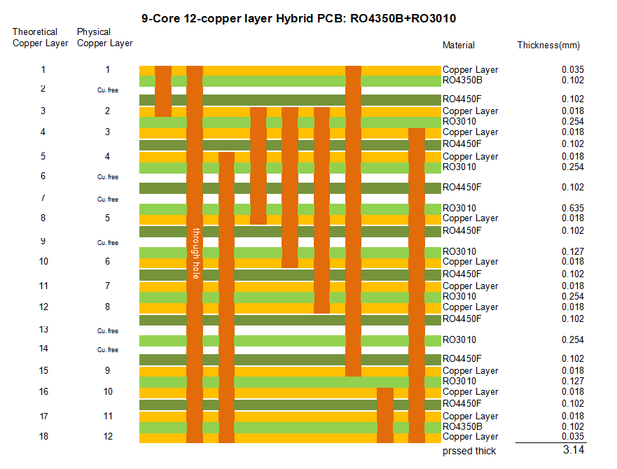
This custom 12-layer mixed dielectric RF multilayer PCB adopts a hybrid stackup combining two classic Rogers high-frequency substrates: 4mil RO4350B core for top and bottom outer layers, matched with 5mil, 10mil and 25mil RO3010 dielectric cores in the middle sections, while RO4450F prepreg is applied as bonding material between all layers. RO4350B and RO3010 hybrid PCB board adopts differentiated copper weight configuration: 1oz copper foil for top and bottom outer signal layers, and 0.5oz copper foil for all inner circuit layers to balance fine-line routing capacity and current carrying capacity.
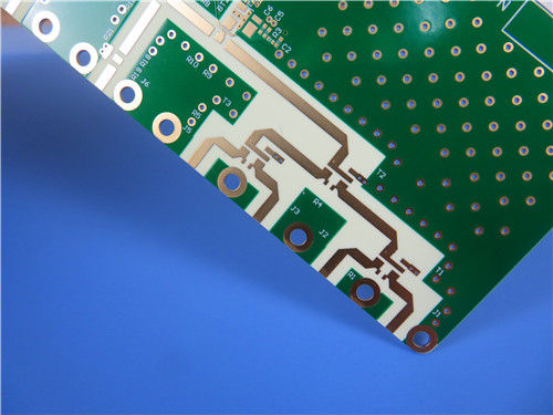
For surface finishing, nickel-free palladium gold plating is adopted without nickel interlayer to deliver superior high-frequency signal performance and stable solderability. RO4350B and RO3010 high-frequency PCB is coated with standard green solder mask with white silk screen legends for clear circuit marking and reliable surface protection. The single unit dimension is 107mm × 91.5mm, with two pieces manufactured on one production panel.
Rogers RO4350B and RO3010 multilayer RF PCB integrates complex multi-group blind hole interconnection architecture to shorten signal transmission paths and reduce high-frequency signal loss. The blind hole types include L1-L2, L2-L5, L2-L6, L2-L8, L1-L9, L10-L12 and L3-L12, which realize flexible cross-layer signal routing for high-density microwave circuit layouts.
2. PCB Basic Specification Table
| Specification Item | Detailed Parameters |
| PCB Layer Count | 12-layer hybrid high-frequency PCB |
| Dielectric Stackup Material | Top 4mil RO4350B core; Middle 5mil/10mil/25mil RO3010 core; Bottom 4mil RO4350B core; Bonding Prepreg: RO4450F |
| Outer Layer Copper Weight | 1oz |
| Inner Layer Copper Weight | 0.5oz |
| Solder Mask & Marking | Green Solder Mask, White Silk Screen Printing |
| Surface Treatment | Nickel-Free Palladium Gold Plating |
| Single Unit Size | 107mm × 91.5mm |
| Panel Layout | 2 PCS per production panel |
| Blind Hole Types | L1-L2, L2-L5, L2-L6, L2-L8, L1-L9, L10-L12, L3-L12 |
3. PCB Stackup Structure Description
This 12-layer mixed dielectric stackup uses RO4350B laminate as the top and bottom outer high-frequency cores with 4mil thickness each, while multiple thickness grades of RO3010 (5mil, 10mil, 25mil) are arranged in the middle inner layers to meet customized impedance and isolation requirements. RO4450F prepreg acts as the interlayer bonding medium to connect all core and copper layers.
The topmost and bottommost copper layers are 1oz outer copper, and all inner signal layers are 0.5oz thin copper for high-density fine-line routing. Multiple sets of blind hole structures penetrate different layer combinations to achieve vertical interconnection between non-adjacent layers, effectively optimizing routing space and minimizing transmission distance for high-frequency RF signals. A stackup diagram can be inserted in this section for visual reference.
4. RO4350B Material Introduction
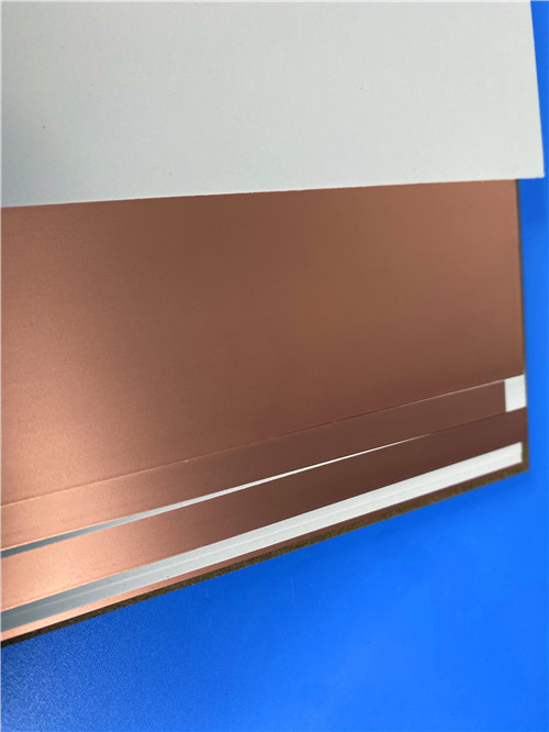
RO4350B laminate belongs to Rogers RO4000 series hydrocarbon ceramic reinforced laminates, which are rigid thermoset substrates distinct from PTFE high-frequency materials. This material is engineered to deliver outstanding high-frequency electrical performance while supporting standard FR-4 mass production processes, balancing premium RF performance and controllable manufacturing costs.
When circuit operating frequency rises above 500MHz, most conventional FR-4 substrates cannot meet low-loss demands, while RO4350B maintains ultra-stable electrical properties across wide frequency bands. It features ultra-low dielectric loss, extremely low temperature coefficient of dielectric constant, and flat Dk performance under varying temperatures and frequencies; optional LoPro foil can further lower signal insertion loss, making it a perfect substrate for broadband RF and microwave circuits.
In terms of thermal and dimensional stability, RO4350B owns a CTE value close to copper, delivering excellent dimensional stability critical for hybrid multi-layer PCB construction. Its low Z-axis thermal expansion guarantees intact plated through holes even under severe thermal shock cycles. With a Tg exceeding 280°C, the material keeps stable expansion characteristics throughout all PCB manufacturing heating processes. Unlike PTFE substrates, RO4350B requires no special sodium etching treatment for vias and fits fully automated copper scrubbing and production equipment.
Rogers RO4350B adopts RoHS-compliant flame retardant formula with UL 94V-0 certification and complies with IPC-4103 standards. It has strong CAF resistance, consistent dielectric tolerance, repeatable impedance control for filter and matching network design, and supports large-volume industrial production with competitive pricing.
5.RO4350B Datasheet
| Property | Typical Value | Direction | Units | Condition | Test Method |
| Dielectric Constant εr (Process) | 3.48 ± 0.05 | Z | — | 10 GHz / 23°C | IPC-TM-650 2.5.5.5 Clamped Stripline |
| Dielectric Constant εr (Design) | 3.66 | Z | — | 8 ~ 40 GHz | Differential Phase Length Method |
| Dissipation Factor tanδ | 0.00370.0031 | Z | — | 10 GHz / 23°C2.5 GHz / 23°C | IPC-TM-650 2.5.5.5 |
| Thermal Coefficient of εr | +50 | Z | ppm/°C | -50°C ~ 150°C | IPC-TM-650 2.5.5.5 |
| Volume Resistivity | 1.2 × 10¹⁰ | — | MΩ•cm | COND A | IPC-TM-650 2.5.17.1 |
| Surface Resistivity | 5.7 × 10⁹ | — | MΩ | COND A | IPC-TM-650 2.5.17.1 |
| Electrical Strength | 31.2 (780) | Z | KV/mm (V/mil) | 0.51mm (0.020”) | IPC-TM-650 2.5.6.2 |
| Tensile Modulus | 16,767 (2,432)14,153 (2,053) | XY | MPa (ksi) | Room Temperature | ASTM D638 |
| Tensile Strength | 203 (29.5)130 (18.9) | XY | MPa (ksi) | Room Temperature | ASTM D638 |
| Flexural Strength | 255 (37) | — | MPa (kpsi) | — | IPC-TM-650 2.4.4 |
| Dimensional Stability | <0.5 | X, Y | mm/m (mils/inch) | After etch + E2 / 150°C | IPC-TM-650 2.4.39A |
| Coefficient of Thermal Expansion | 101232 | XYZ | ppm/°C | -55°C ~ 288°C | IPC-TM-650 2.4.41 |
| Tg (Glass Transition Temperature, TMA Method A) | >280 | — | °C | Method A | IPC-TM-650 2.4.24.3 |
| Td (Decomposition Temperature, TGA) | 390 | — | °C | TGA Test | ASTM D3850 |
| Thermal Conductivity | 0.69 | — | W/m·K | 80°C | ASTM C518 |
| Moisture Absorption | 0.06 | — | % | 48 hrs immersion, 0.060” sample, 50°C | ASTM D570 |
| Density | 1.86 | — | g/cm³ | 23°C | ASTM D792 |
| Copper Peel Strength | 0.88 (5.0) | — | N/mm (pli) | After solder float, 1 oz. EDC Foil | IPC-TM-650 2.4.8 |
| Flammability | V-0 | — | — | — | UL 94 |
| Lead-Free Process Compatible | Yes | — | — | — | — |