


 Home
Home
Is Your Traditional PCB Holding Back Your Design? When to Switch to HDI PCB
 February 27,2026
In the era of miniaturized, high-performance electronics—from 5G smartphones to autonomous vehicle sensors—High-Density Interconnect (HDI) PCBs have become indispensable. Unlike traditional PCBs, HDI technology uses microvias, blind vias, and fine-pitch routing to pack more functionality into smaller spaces. Below are the core advantages that make HDI PCBs the top choice for global electronics manufacturers, along with a clear comparison to traditional options.
1.Key Advantages of HDI PCBs
Miniaturization & Space Savings: HDI PCBs leverage laser-drilled microvias (as small as 0.075mm) and fine line widths (down to 50 microns) to boost wiring density by over 30% compared to traditional PCBs. This means more components and connections can fit in the same or smaller board area, enabling slimmer, lighter devices like wearables and compact medical monitors .
Superior Signal Integrity: Shorter signal paths and eliminated via stubs reduce signal loss, delay, and electromagnetic interference (EMI). This is critical for high-frequency applications such as 5G communication and automotive radar, where stable signal transmission directly impacts performance .
Enhanced Reliability: Laser-drilled microvias have fewer manufacturing defects and better resistance to thermal expansion (CTE) changes than traditional plated through-holes. The use of blind and buried vias also reduces mechanical stress on the board, extending the lifespan of devices in harsh environments like aerospace or industrial settings .
Cost-Efficiency in the Long Run: While initial production costs may be higher, HDI PCBs reduce the number of required layers, cut material waste, and lower repair/replacement costs due to their durability. For high-volume applications like smartphones, these savings add up significantly .
Related Product Example:
If you are interested in high-performance HDI RF PCBs, you may refer to the Rogers RO4350B 8-Layer 1.6mm HDI RF PCB, which combines HDI technology with high-frequency material properties, making it suitable for RF applications with stringent signal integrity requirements.
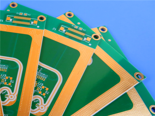
8-Layer 1.6mm RO4350B HDI PCB
2.HDI PCB vs. Traditional PCB: Quick Comparison
Feature |
HDI PCB |
Traditional PCB |
Wiring Density |
High (30%+ higher than traditional) |
Low |
Via Size |
Microvias (0.075–0.15mm) |
Large (≥0.3mm) |
Signal Loss |
Minimal (short signal paths) |
Significant (long signal paths) |
Device Compatibility |
Ideal for 5G, wearables, ADAS |
Suitable for basic electronics |
Long-Term Cost |
Cost-effective (fewer repairs, less material) |
Higher (more replacements, more material) |
3.HDI vs. Traditional PCB Selection Guide
Unsure which PCB technology to choose? This guide helps you make a clear decision.
When HDI is Essential
Choose HDI if your design meets any of these critical requirements:
High Frequency/Speed: For example, 5G/6G RF, automotive radar, or high-speed computing.
Extreme Miniaturization: Such as in smartphones or wearables that demand maximum wiring density.
Harsh Environments: When high reliability under thermal stress, vibration, or extreme conditions is required.
Comparison: Three HDI PCB Layer Configurations
When a Traditional PCB is Sufficient
Opt for a traditional PCB if your project is defined by the following:
Cost Sensitivity & Simplicity: For prototypes, low-to-medium volume runs, or designs with ample board space.
Basic Performance Needs: When the design uses low-frequency components and operates in stable environments.
Fast Time-to-Market: For straightforward designs where manufacturing simplicity is an advantage.
Quick Decision Checklist
Answer these questions to guide your choice:
Is my signal frequency above 1 GHz? (Yes → HDI)
Is product size/weight a critical constraint? (Yes → HDI)
Is minimizing initial unit cost the top priority? (Yes → Traditional)
Will the product face extreme operational stress? (Yes → HDI)
4.Concluding Remarks
From consumer electronics to industrial automation, HDI PCBs drive innovation by solving the dual challenges of miniaturization and performance. As 6G and AI devices emerge, their role as the backbone of electronics will only strengthen.
In summary, HDI PCBs are indispensable for cutting-edge applications demanding maximum performance and size reduction, while traditional PCBs remain the reliable, cost-effective foundation for established functionalities. The future of electronics is built on this complementary technological foundation.
Founded in 2003, Shenzhen Bicheng Electronics Technology Co., Ltd is an established high frequency PCB supplier and exporter in Shenzhen, China, serving customers worldwide.
We are devoted to delivering high-frequency PCB products and solutions of the highest quality, along with customized service. Get in touch with us to start your project !
Visit https://www.bicheng-enterprise.com to learn more.