
 Home
Home
What is PCBA? A Complete Guide to Printed Circuit Board Assembly
Printed Circuit Board Assembly (PCBA) refers to the finished product after electronic components—such as resistors, capacitors, integrated circuits (ICs), connectors, and more—are fully mounted and soldered onto a printed circuit board (PCB). Once all necessary components are installed, the board becomes a PCBA: a fully functional circuit ready to perform its intended tasks. In short, PCBA represents the final, operational electronic circuit created by assembling components onto a PCB.
1.The Assembly Process: From Bare Board to Functional PCBA
The transformation from a bare PCB to a PCBA is known as the PCB assembly process. This involves multiple stages and is commonly achieved using two primary technologies:
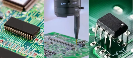
Picture 1: SMT、SMD and THT
2.Surface Mount Technology (SMT):
In SMT assembly, components—referred to as Surface Mount Devices (SMDs)—are placed directly onto the PCB’s solder pads. A solder paste (a mix of solder and flux) is first applied to the pads, followed by precise component placement using automated pick-and-place machines. The board then passes through a reflow oven, where the solder melts, permanently bonding the components to the pads. SMT is widely used in modern electronics due to its support for high component density and the ability to assemble both sides of the PCB.
3.Through-Hole Technology (THT):
THT involves inserting components with wire leads—such as traditional resistors, capacitors, or connectors—into pre-drilled holes on the PCB. The leads are then soldered, either manually or using wave soldering equipment, onto pads located on the opposite side. THT offers strong mechanical bonds, making it suitable for components subjected to physical stress, though it generally allows for lower component density compared to SMT.
4.Mixed Assembly:
Many PCBAs combine both SMT and THT. For example, while most small components (ICs, chips, resistors) are surface-mounted, larger parts like connectors or electrolytic capacitors may be through-hole mounted. This hybrid approach may require multiple assembly steps.
5.Typical PCBA Workflow Steps
A standard PCBA process includes solder paste printing, component placement, soldering (reflow for SMT, wave soldering for THT), inspection, and testing. Automated Optical Inspection (AOI) and X-ray inspection (essential for hidden solder joints like those in BGA chips) help detect soldering defects. Finally, each PCBA typically undergoes electrical tests—such as In-Circuit Test (ICT) or functional validation—to ensure performance and reliability.
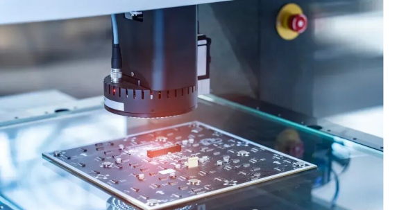
Picture 2: AOI in Process on a PCB
6.Why PCBA Matters
The PCBA is what brings electronic devices to life. For instance, the PCB inside a smartphone only becomes a functional motherboard—capable of powering the device—once all chips and passive components are soldered on. While people often refer to an assembled board informally as a "PCB," the technically accurate term for a populated, working board is PCBA (sometimes also called PCA, or Printed Circuit Assembly).
7.Key Differences: PCB vs. PCBA
Although closely related, PCB and PCBA represent different stages in electronics manufacturing:
Aspect |
PCB (Bare Board) |
PCBA (Assembled Board) |
Definition |
Unpopulated board with copper traces |
PCB with all electronic components mounted |
Function |
Provides mechanical base & connectivity |
Performs specific electronic functions |
Components |
None |
Resistors, capacitors, ICs, connectors, etc. |
Manufacturing Process |
Etching, drilling, solder mask application |
Component placement, soldering, testing |
Testing |
Continuity & short-circuit checks |
ICT, functional, and AOI/X-ray inspection |
Application |
Prototyping, circuit validation |
Final products: phones, computers, IoT devices |
A simple way to remember: PCB + Components + Soldering = PCBA.
8.Design Workflow & Real-World Use
The electronics design workflow clearly separates the PCB and PCBA stages. Engineers first design the circuit and board layout using Electronic Design Automation (EDA) software. Once the PCB design is finalized, the bare board is fabricated, and components are assembled—either in-house or by a specialized PCBA service provider.
Notably, many developers and hobbyists today use off-the-shelf PCBAs—such as Arduino or Raspberry Pi boards—as building blocks in larger projects. These modules are themselves complete PCBAs, built around a core PCB.
9.PCBA Cost Considerations
The total cost of a PCBA includes not only the bare PCB but also component procurement, assembly labor (or machine operation), soldering materials, and comprehensive testing.
10.Summary
PCBA is the result of merging a bare PCB with electronic components through precise assembly techniques such as SMT and THT, followed by rigorous inspection. It transforms a passive substrate into the operational "heart" of an electronic device. As the central functional unit, PCBA bridges circuit design and real-world application, where balancing cost, precision, and reliability directly defines an electronic product’s performance and market success.