

 Home
Home
What Are the Classifications of Holes in Printed Circuit Boards?
IIn multilayer printed circuit boards (PCBs), vias are fundamental components. Drilling these holes typically accounts for 30% to 40% of the total PCB manufacturing cost, making via design a critical aspect of the PCB layout process.
1.Understanding Basic Via Classifications
In simple terms, any hole on a PCB can be referred to as a via. Functionally, vias fall into two main categories: those for electrical interconnection between layers and those for component mounting or board positioning. From a manufacturing standpoint, these vias are further classified into three primary types: Blind Vias, Buried Vias, and Through-Hole Vias.
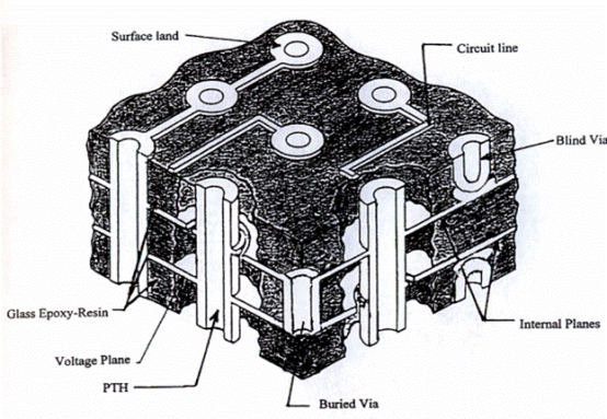
Figure 1: PCB Layer Structure and Via Types
2.Blind Vias: Connecting Surface to Inner Layers
Blind Vias connect an outer layer (top or bottom) to one or more adjacent inner layers without passing through the entire board. The depth of a blind via is precisely controlled and typically does not exceed a certain ratio relative to the hole diameter.
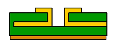
Figure 2: Blind Via Structure
3.Buried Vias: Exclusive Internal Connections
Buried Vias are located entirely within the inner layers of the PCB and do not reach either outer surface. Both blind and buried vias are formed using sequential lamination processes before the final board layers are pressed together, allowing for complex, high-density interconnections between specific internal layers.
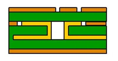
Figure 3: Buried Via Structure
4.Through-Hole Vias: The Most Common Solution
The third type is the Through-Hole Via. This via passes through the entire thickness of the circuit board. It can be used for internal layer interconnection or as a mounting hole for through-hole components. Due to their simpler manufacturing process and lower cost, through-hole vias are the most common type used in PCBs, while blind and buried vias are typically reserved for advanced, space-constrained designs.
Unless otherwise specified, the term "via" generally refers to a through-hole via. From a design perspective, a via consists of two main parts: the central drill hole and the surrounding pad area. The dimensions of these two elements define the effective size of the via.
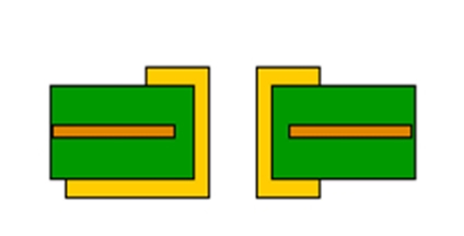
Figure 4: Through-Hole Via Structure
5.Navigating Technical and Economic Constraints in Via Sizing
In high-speed, high-density PCB design, engineers naturally prefer smaller vias. Minimizing via size conserves valuable routing space. Furthermore, smaller vias possess lower parasitic capacitance, enhancing their suitability for high-frequency and high-speed signals. However, reducing via size introduces both economic and technical challenges. Smaller holes require longer drilling times and increase risks of drill bit breakage and positional inaccuracy. Additionally, achieving uniform copper plating on high-aspect-ratio hole walls becomes increasingly difficult. Inconsistent plating thickness—particularly thin or porous sections in the barrel center—can severely compromise mechanical reliability and long-term fatigue life, potentially leading to field failures. These manufacturing limitations, combined with rising costs, establish practical boundaries for via miniaturization, demanding careful consideration of performance requirements against production feasibility.
6.Strategic Via Selection for Optimal Design
Understanding the different types of PCB vias—Blind, Buried, and Through-Hole—is essential for optimizing both the performance and cost-effectiveness of your board design. While smaller through-hole vias are ideal for high-speed routing, designers must balance this against manufacturing capabilities and cost constraints. Choosing the right via type and size in collaboration with your PCB manufacturer ensures a robust, reliable, and economically viable product.