

 Home
-Newly shipped PCBs-
Rogers 6-Layer High-Frequency PCB with 0.203mm RO4003C laminate and Advanced Back Drilling Technology for 5G, Automotive Radar and Aerospace Applications
Home
-Newly shipped PCBs-
Rogers 6-Layer High-Frequency PCB with 0.203mm RO4003C laminate and Advanced Back Drilling Technology for 5G, Automotive Radar and Aerospace Applications
Rogers 6-Layer High-Frequency PCB with 0.203mm Rogers RO4003C laminate and Advanced Back Drilling Technology for 5G, Automotive Radar and Aerospace Applications
Printed Circuit Boards are custom-made products; the images and specifications provided are for reference only.
1. Introduction : Rogers RO4003C-Based High-Frequency PCB
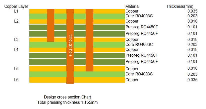
This 6-layer high-frequency Printed Circuit Board is engineered using Rogers RO4003C hydrocarbon ceramic laminate—a material that combines exceptional electrical performance with standard epoxy/glass (FR-4) processing economics. Designed for demanding RF and microwave applications up to millimeter-wave frequencies, Rogers 6-layer RO4003C circuit board features a hybrid construction with 0.203mm RO4003C cores on the top, middle, and bottom layers, bonded by Rogers RO4450F prepreg material. The board incorporates precision back drilling techniques to eliminate via stubs for L1-L3 and L1-L5 transitions, ensuring optimal signal integrity at high frequencies. With immersion gold (ENIG) surface finish, green solder mask with white legend on both sides, and controlled impedance capabilities, RO4003C PCB is purpose-built for telecommunications infrastructure, aerospace radar systems, and advanced test equipment where low signal loss and phase stability are critical.
2. Understanding Back Drilling Technology
Back drilling, also known as controlled-depth drilling, is a specialized PCB manufacturing process used to remove the unused portion of a plated through-hole via that extends beyond the required interconnection layers . In high-frequency applications, these unused via stubs act as antennas, causing signal reflections, impedance discontinuities, and insertion loss that degrade signal integrity .
2.1 How Back Drilling Works
The process involves drilling out the non-functional stub portion of a via to a precisely controlled depth, removing the excess copper barrel that would otherwise cause signal degradation . For this PCB design, back drilling is implemented for L1-L3 and L1-L5 transitions, ensuring that signal paths remain clean and uninterrupted through the critical upper layers where high-frequency signals travel.
2.2 Benefits of Back Drilling
Benefit |
Description |
Impact on Performance |
Stub Elimination |
Removes excess via barrel length beyond signal layers |
Reduces signal reflections by eliminating resonant structures |
Impedance Control |
Maintains consistent characteristic impedance |
Improves signal integrity for >10 GHz designs |
Insertion Loss Reduction |
Minimizes energy loss in transmission paths |
Enhances overall circuit efficiency |
EMI Reduction |
Decreases electromagnetic interference from via stubs |
Improves system noise performance |
3. PCB Specifications Overview
RO4003C 6-layer high-frequency PCB is manufactured to precise specifications, ensuring consistent performance for critical RF and microwave applications.
Feature |
Specification |
Technical Note |
Layer Count |
6 Layers |
Optimized for complex RF routing and power distribution |
Core Material |
Rogers RO4003C™ (0.203mm each layer) |
Glass-reinforced hydrocarbon/ceramic laminate |
Prepreg Material |
Rogers RO4450F™ (2 sheets between cores) |
Compatible bonding material for multilayer construction |
Total Thickness |
1.174 mm (finished) |
Precision-controlled lamination |
Copper Weight (Outer) |
1 oz (35 µm) finished |
Optimized for outer layer signal transmission |
Copper Weight (Inner) |
0.5 oz (17.5 µm) finished |
Balanced for inner layer routing requirements |
Surface Finish |
Immersion Gold (ENIG) |
Excellent solderability and corrosion resistance |
Solder Mask & Legend |
Green Mask, White Legend (Top & Bottom) |
High contrast for automated optical inspection |
Board Dimensions |
92.5 x 77.3 mm (per piece) |
Compact form factor for integrated assemblies |
Special Process |
Back Drilling L1-L3, L1-L5 |
Stub elimination for critical signal paths |
4. In-Depth: Rogers RO4003C Material Technology
Rogers RO4003C represents a breakthrough in high-frequency laminate technology, offering electrical properties approaching those of PTFE/glass materials while maintaining the processability of standard epoxy/glass systems .
4.1 Key Material Properties
Property |
Value |
Conditions |
Dielectric Constant (Dk) |
3.38 ± 0.05 |
@10 GHz, process control value |
Design Dk |
3.55 |
@10 GHz, for impedance calculations |
Dissipation Factor (Df) |
0.0027 |
@10 GHz, 23°C |
Thermal Coefficient of Dk |
+40 ppm/°C |
-50°C to 150°C |
Volume Resistivity |
1.7 x 10¹⁰ Mohm |
Typical |
Surface Resistivity |
4.2 x 10⁹ Mohm |
Typical |
Water Absorption |
0.04% |
D48/50% |
Thermal Conductivity |
0.71 W/m/°K |
50°C, ASTM D5470 |
CTE (X-axis) |
11 ppm/°C |
-55°C to 288°C |
CTE (Y-axis) |
14 ppm/°C |
-55°C to 288°C |
CTE (Z-axis) |
46 ppm/°C |
-55°C to 288°C |
Peel Strength (1 oz ED) |
6.0 lbs/in (1.05 N/mm) |
Typical |
Density |
1.8 g/cm³ |
Typical |
Flammability Rating |
NON FR (UL94) |
Note: Not UL 94 V-0 rated |
4.2 Key Advantages of RO4003C
Exceptional Electrical Performance: Tightly controlled dielectric constant (Dk 3.38 ± 0.05) and low dissipation factor (0.0027 at 10 GHz) ensure minimal signal loss and phase stability across frequency .
FR-4 Compatible Processing: Unlike PTFE-based microwave materials, RO4003C requires no special via treatments or handling procedures, allowing fabrication using standard epoxy/glass processes at significantly lower cost .
Ideal for Multilayer Constructions: The material's mechanical properties and compatibility with standard lamination processes make it excellent for complex multilayer board (MLB) designs .
Dimensional Stability: Low Z-axis expansion (46 ppm/°C) and CTE matching with copper ensure reliability through thermal cycling .
Low Moisture Absorption: At just 0.04%, the material maintains stable electrical performance even in humid environments .
Thermal Performance: Glass transition temperature exceeding 280°C and decomposition temperature above 425°C support lead-free assembly processes .
4.3 Typical Applications
Rogers RO4003C finds widespread use in demanding high-frequency applications :
Wireless Communications: 5G base station antennas, power amplifiers, filters, and combiners
Automotive Radar: 77 GHz millimeter-wave radar systems for ADAS and autonomous vehicles
Aerospace & Defense: Satellite communication systems, radar arrays, and avionics
Test & Measurement: Microwave test equipment and precision measurement instruments
RF Identification: High-performance RFID readers and tags
Point-to-Point Microwave: Backhaul communication systems
Broadcast Systems: LNBs for satellite television reception
5. Design Considerations for Optimal Performance
5.1 Impedance Control
The stable Dk of RO4003C (3.38 ± 0.05) enables precise impedance control for 50-ohm and 100-ohm differential transmission lines. For microstrip structures on 0.203mm core material with 1 oz copper, typical 50-ohm line widths range from 0.35mm to 0.40mm, depending on final stack-up configuration .
5.2 Back Drilling Precision
For L1-L3 and L1-L5 back drilling, depth control tolerance of ±0.05mm is maintained to ensure complete stub removal without compromising the target layer connections. This precision is essential for maintaining signal integrity in multi-gigahertz designs .
5.3 Thermal Management
While RO4003C offers thermal conductivity of 0.71 W/m/°K, high-power applications benefit from thermal via arrays and consideration of copper plane distribution for effective heat spreading .
5.4 Hybrid Stack-Up Possibilities
For cost-optimized designs, RO4003C can be combined with FR-4 inner layers, though careful stack-up design and process control are required to manage CTE differences and prevent warpage .
6. Conclusion
This 6-layer high-frequency PCB, constructed with Rogers RO4003C cores and RO4450F prepreg, represents an optimal balance of electrical performance and manufacturing efficiency. The material's tightly controlled dielectric constant (3.38 ± 0.05) and low dissipation factor (0.0027) ensure minimal signal loss through 10 GHz and beyond, while its compatibility with standard FR-4 processing eliminates the cost premiums associated with traditional microwave laminates . The implementation of precision back drilling for L1-L3 and L1-L5 transitions eliminates via stub effects that would otherwise degrade signal integrity at high frequencies. With immersion gold finish, green solder mask, and controlled impedance capabilities, this PCB is engineered to meet the demanding requirements of 5G infrastructure, automotive radar systems, aerospace communications, and advanced test equipment where signal purity and reliability are non-negotiable.
Founded in 2003, Shenzhen Bicheng Electronics Technology Co., Ltd is an established high frequency PCB supplier and exporter in Shenzhen, China, serving customers worldwide.
We are devoted to delivering high-frequency PCB products and solutions of the highest quality, along with customized service. Get in touch with us to start your project !
Visit https://www.bicheng-enterprise.com to learn more.