


 Home
-
Newly shipped PCBs
-
Panasonic MEGTRON 6 14-layer 1.64mm High Speed PCB with ENEPIG Finish for Networking & Wireless Communication
Home
-
Newly shipped PCBs
-
Panasonic MEGTRON 6 14-layer 1.64mm High Speed PCB with ENEPIG Finish for Networking & Wireless Communication
Panasonic MEGTRON 6 14-layer 1.64mm High Speed PCB with ENEPIG Finish for Networking & Wireless Communication
Printed Circuit Boards are custom-made products; the images and specifications provided are for reference only.
1. Introduction
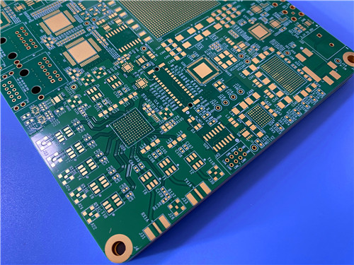
This high-performance 14-layer multilayer PCB adopts Panasonic MEGTRON 6 ultra-low loss substrate, finished with a total board thickness of 1.64mm. It adopts differentiated copper weight design: 1oz copper foil for outer signal layers and 0.5oz copper foil for all inner layers to balance current carrying capacity and fine-line routing capacity. The surface treatment adopts nickel-palladium-gold (ENEPIG), matched with green solder mask and white silk screen marking to achieve clear circuit identification, outstanding oxidation resistance and long-term reliability. The finished single unit dimension is 178.8mm × 169mm, arranged in a 2×2 panel layout with 4 pieces per panel. 5mm wide process edges are reserved on all four sides of the entire panel to meet automated production, routing and testing requirements. This PCB strictly complies with IPC-3 industrial standards, and all through holes adopt resin plugging process following IPC-4761 TYPE VII specification to eliminate hollow holes, strengthen interlayer bonding and improve soldering stability. Customized precise impedance control is configured for microstrip and stripline transmission lines to guarantee stable signal integrity under high-speed signal transmission.
2.PCB Basic Specification Table
Specification Item |
Detailed Parameters |
PCB Layer Count |
14-layer Multilayer Board |
Base Material |
Panasonic MEGTRON 6 (R-5775 Laminate & R-5670 Prepreg) |
Finished Board Thickness |
1.64mm |
Outer Layer Copper Weight |
1oz |
Inner Layer Copper Weight |
0.5oz |
Surface Finish |
ENEPIG (Nickel Palladium Gold) |
Solder Mask & Marking |
Green Solder Mask, White Silk Screen |
Single Unit Size |
178.8mm × 169mm |
Panel Layout |
2×2 arrangement, 4 PCS per panel |
Process Edge |
5mm width on four sides |
Compliance Standard |
IPC-3 Standard |
Plug Hole Spec |
Resin Plug Hole, IPC-4761 TYPE VII |
Impedance Control |
Custom microstrip & stripline impedance design |
3. Impedance Control Parameters
Microstrip
- 50Ω single-end trace: line width 0.2mm
- 100Ω differential pair: line width 0.1mm, space 0.101mm
Stripline
- 50Ω single-end trace: line width 0.1mm
- 100Ω differential pair: line width 0.2mm, space 0.102mm
4. PCB Stackup Structure Description
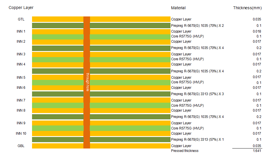
This 14-layer high-speed PCB is built with Panasonic MEGTRON 6 R-5775 core laminates and matching R-5670 prepregs with ultra-low Dk/Df performance. The overall stackup structure takes the 1oz outer copper layer as the top signal layer with microstrip impedance traces, and multiple groups of 0.5oz inner copper layers sandwiched between MEGTRON 6 dielectric materials. Key inner layers are designed with stripline impedance-controlled traces for high-speed differential and single-end signals. All inner layers are isolated by low-loss MEGTRON 6 prepreg to reduce signal attenuation and crosstalk. The bottom outer layer uses 1oz copper for external connection, forming a symmetric, thermally stable stackup that supports HDI fabrication and high-temperature reflow cycles. A material stackup schematic can be inserted at this section for visual reference.
5. MEGTRON 6 Material Introduction
Panasonic MEGTRON 6 series covers multiple variants including MEGTRON 6(G), MEGTRON 6(K) and MEGTRON 6(N), which have become classic benchmark ultra-low loss substrates in the PCB industry. The product system consists of R-5775 core laminate and supporting R-5670 prepreg, available with low Dk special glass cloth and standard E-glass cloth versions. MEGTRON 6 material features ultra-low dielectric loss and superior heat resistance, delivering premium performance for high-speed circuit transmission. It also owns outstanding HDI manufacturing adaptability and stable thermal properties, which can well cope with complex multi-layer pressing, drilling and desmear processes in mass production. Tailored for high-frequency and high-speed scenarios, the material minimizes signal loss during broadband signal transmission and maintains consistent electrical performance across wide frequency ranges.
.jpg)
6. MEGTRON 6 Process Guideline
This official Panasonic process guideline provides standardized full-flow manufacturing instructions for R-5775 laminate and R-5670 prepreg, covering all core production steps for high-speed MEGTRON 6 PCBs.
Material Storage Requirements
Laminate panels must be stored flat in cool, dry surroundings without bending or surface scratching; original packaging is recommended for long-term storage. Prepreg needs controlled storage below 23°C with RH ≤50%. For long-term stock, store prepreg at 5°C, and sealed all opened bags immediately. Cumulative exposure time under normal environment shall not exceed 8 hours unless agreed by supplier.
Surface & Inner Layer Treatment
Shiny copper surfaces adopt standard chemical or mechanical cleaning; reverse treated copper only uses chemical cleaning. Inner layer bonding supports black oxide, brown oxide or organic alternative peroxide/sulfuric acid etching treatment; black oxide requires peel strength verification before mass use. Fully bake finished inner layers at 105°C for 20–30 minutes to eliminate surface and absorbed moisture.
Drilling Parameters
Drilling parameters vary by hole diameter, layer count and panel thickness. The guideline lists complete spindle speed, feed rate, chip load and drill bit life ranges for hole sizes from 0.20mm to 0.90mm. Recommended practices include lubricated aluminum entry sheets, high helix angle drill bits and peck drilling for tiny holes, with spindle speed adjusted to keep cutting velocity between 100–150 m/min. Fixed positioning accuracy test data for φ0.30 drill holes is also attached for reference.
Lamination Process
Lamination temperature, pressure and vacuum settings are determined by multilayer package thickness. Standard heating rate is 2.0–4.0°C/min, target product temperature over 185°C held for 75 minutes, working pressure 3.0–4.0MPa with 0.5MPa pre-pressure for 20 minutes, and vacuum maintained below 100torr and stopped after 30 minutes heating.
Desmear Treatment
Permanganate desmear needs twice the process duration of standard FR-4 because R-5775/R-5670 have lower resin weight loss ratio (0.2–0.4 vs FR-4’s 1.0). Plasma desmear only requires half the FR-4 processing time. For hybrid boards mixed with FR-4, combine short-time plasma and permanganate desmear without swelling step.
Surface Finishing Compatibility
MEGTRON 6 supports silver plating, tin plating, direct gold plating and OSP directly. If ENEPIG or ENIG nickel plating is required, pre-bake the board at 150°C for 5 hours or store at room temperature for one week to avoid plating defects.
Pre-Use & Safety Notices
Customers must conduct independent performance testing to verify material suitability before formal mass adoption. Formal delivery specifications shall be signed by both parties as priority execution standards. Product appearance and specifications are subject to change without prior notice for technical upgrade. All materials are dedicated electronic circuit substrates and cannot be applied to other fields. Global sales and technical support contact information for Panasonic’s regional branches are listed in the complete guideline for technical consultation.
7. MEGTRON 6 Application Fields
Benefiting from ultra-low dielectric loss, stable high-frequency electrical performance, excellent HDI manufacturability and strong thermal resistance, MEGTRON 6 series substrates are widely adopted in high-end high-speed electronic hardware. Typical application scenarios include mobile communication terminals, network switches, routers, wireless base station equipment and other high-frequency broadband signal devices. It is the preferred core dielectric material for 14-layer and above high-layer-count high-speed multilayer PCBs that demand minimal signal attenuation and long-term thermal stability.
8.MEGTRON 6 Datasheet
Table 1: Single Item Technical Specifications of R-5775/R-5670 Substrate
Property |
Units |
Test Method |
Condition |
Typical Value |
THERMAL PROPERTIES |
|
|
|
|
Glass Transition Temp (Tg) |
°C |
DSC |
As received |
185 |
Glass Transition Temp (Tg) |
°C |
DMA |
As received |
210 |
Thermal Decomposition Temp (Td) |
°C |
TGA |
As received |
410 |
Time to Delaminate (T288) – Without Cu |
Min |
IPC TM-650 2.4.24.1 |
As received |
> 120 |
Time to Delaminate (T288) – With Cu |
Min |
IPC TM-650 2.4.24.1 |
As received |
> 120 |
CTE α1 (X-axis, <Tg) |
ppm/°C |
IPC TM-650 2.4.24 |
< Tg |
14–16 |
CTE α1 (Y-axis, <Tg) |
ppm/°C |
IPC TM-650 2.4.24 |
< Tg |
14–16 |
CTE α1 (Z-axis, <Tg) |
ppm/°C |
IPC TM-650 2.4.24 |
< Tg |
45 |
CTE α2 (Z-axis, >Tg) |
ppm/°C |
IPC TM-650 2.4.24 |
> Tg |
260 |
ELECTRICAL PROPERTIES |
|
|
|
|
Volume Resistivity |
MΩ·cm |
IPC TM-650 2.5.17.1 |
C-96/35/90 |
1×10⁹ |
Surface Resistivity |
MΩ |
IPC TM-650 2.5.17.1 |
C-96/35/90 |
1×10⁸ |
Dielectric Constant (Dk) @ 1GHz |
— |
IPC TM-650 2.5.5.9 |
C-24/23/50 |
3.40 |
Dielectric Constant (Dk) @ 13GHz |
— |
*Note 1 |
C-24/23/50 |
3.34 |
Dissipation Factor (Df) @ 1GHz |
— |
IPC TM-650 2.5.5.9 |
C-24/23/50 |
0.002 |
Dissipation Factor (Df) @ 13GHz |
— |
*Note 1 |
C-24/23/50 |
0.0037 |
PHYSICAL PROPERTIES |
|
|
|
|
Water Absorption |
% |
IPC TM-650 2.6.2.1 |
D-24/23 |
0.14 |
Peel Strength (1oz H-VLP Foil) |
kN/m |
IPC TM-650 2.4.8 |
As received |
0.8 |
Flammability |
— |
UL |
C-48/23/50 |
94V-0 |
Table 2: Performance Comparison Table of Full R-5775/R-5670 Series Models
Property |
R-5775(K)/R-5670(K) |
R-5775(N)/R-5670(N) |
R-5775(G)/R-5775(G) |
Tg (DSC) |
185 °C |
185 °C |
185 °C |
Tg (DMA) |
210 °C |
210 °C |
210 °C |
Td (Thermal Decomposition) |
410 °C |
410 °C |
410 °C |
T288 (Without Cu) |
>120 min |
>120 min |
>120 min |
T288 (With Cu) |
>120 min |
>120 min |
>120 min |
CTE X/Y-axis (α1, <Tg) |
14–16 ppm/°C |
14–16 ppm/°C |
14–16 ppm/°C |
CTE Z-axis (α1, <Tg) |
45 ppm/°C |
45 ppm/°C |
45 ppm/°C |
CTE α2 Z-axis (>Tg) |
260 ppm/°C |
260 ppm/°C |
260 ppm/°C |
Thermal Conductivity |
0.42 W/m·K |
0.42 W/m·K |
0.42 W/m·K |
Volume Resistivity |
1×10⁹ MΩ·cm |
1×10⁹ MΩ·cm |
1×10⁹ MΩ·cm |
Surface Resistivity |
1×10⁸ MΩ |
1×10⁸ MΩ |
1×10⁸ MΩ |
Dk @ 1 GHz |
3.4 |
3.4 |
3.4 |
Dk @ 10 GHz |
— |
— |
— |
Dk @ 12 GHz |
3.4 |
3.4 |
3.4 |
Df @ 1 GHz |
0.002 |
0.002 |
0.002 |
Df @ 10 GHz |
— |
— |
— |
Df @ 12 GHz |
0.004 |
0.004 |
0.004 |
Water Absorption |
0.14% |
0.14% |
0.14% |
Poisson's Ratio |
0.2 |
0.2 |
0.2 |
Flexural Modulus MD (Warp) |
19 GPa |
19 GPa |
19 GPa |
Flexural Modulus TD (Fill) |
18 GPa |
18 GPa |
18 GPa |
Peel Strength (1 Oz H-VLP Cu) |
0.8 kN/m |
0.8 kN/m |
0.8 kN/m |
Flammability |
94V-0 |
94V-0 |
94V-0 |
9. Summary
This customized 14-layer 1.64mm multilayer PCB is manufactured with Panasonic MEGTRON 6 ultra-low loss high-speed material, combining 1oz outer copper and 0.5oz inner copper design with reliable ENEPIG surface finishing. Produced in a 2×2 panel layout with reserved 5mm process edges on four sides, the product strictly follows IPC-3 standards and IPC-4761 TYPE VII resin plug hole technology, paired with full-range microstrip and stripline impedance control to guarantee superior high-speed signal integrity. Supported by the complete standardized Panasonic MEGTRON 6 production process specification, the board delivers stable thermal performance, low signal loss and high interlayer reliability, fully matching the strict manufacturing demands of networking, wireless and mobile high-speed communication equipment.
Tags: 14-layer 1.64mm PCB, MEGTRON 6 PCB, Panasonic R-5775 laminate, R-5670 prepreg, ENEPIG PCB, High Speed Low Loss PCB, Resin Plug Hole IPC-4761 TYPE VII, Impedance Control Multilayer PCB, HDI Communication PCB, Wireless Network PCB, Ultra Low Dk PCB, High Thermal Resistance PCB, IPC-3 Standard PCB, High Frequency PCB, Networking Equipment PCB