


 Home
-
Newly shipped PCBs
-
FSD1020T 0.508mm 2-Layer Rigid PCB with Resin Plugged and Capped Holes for High-Power RF & Industrial Electronics
Home
-
Newly shipped PCBs
-
FSD1020T 0.508mm 2-Layer Rigid PCB with Resin Plugged and Capped Holes for High-Power RF & Industrial Electronics
FSD1020T 0.508mm 2-Layer Rigid PCB with Resin Plugged and Capped Holes for High-Power RF & Industrial Electronics
Printed Circuit Boards are custom-made products; the images and specifications provided are for reference only.
1. Introduction of FSD1020T PCB
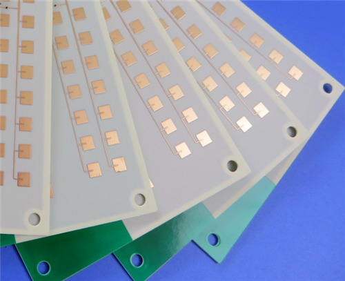
This 2-layer rigid PCB adopts premium FSD1020T carbon-hydrogen nano-ceramic composite substrate with a core thickness of 0.508mm. Customized to dimensions of 96mm × 47mm (1 piece), the board uses 1oz copper on outer layers and features customized solder mask and silkscreen design: green solder mask without silkscreen on the top side, while the bottom side comes with no solder mask and no silkscreen. It is finished with enhanced ENIG surface treatment at 170% coverage, and equipped with 0.4mm holes processed via professional resin plugging and capping technology.
Combining low-loss dielectric performance, reliable insulation and excellent machinability, FSD1020T PCB is engineered for high-current and high-power RF circuits. Every finished board undergoes strict quality inspection to ensure stable and consistent performance, serving as a reliable circuit solution for industrial monitoring, navigation, UAV and transportation-related electronic systems.
2. Key Features of FSD1020T PCB
- Adopts high-performance FSD1020T carbon-hydrogen nano-ceramic composite substrate
- 2-layer rigid structure with 0.508mm standard core thickness and 1oz outer copper weight for stable current conduction
- 0.4mm holes processed with resin plugging and capping, improving hole reliability and anti-pressure capability
- Enhanced 170% ENIG surface finish for superior corrosion resistance and solderability
- Custom surface coating: top layer with green solder mask and no silkscreen; bottom layer without solder mask and silkscreen
- High Tg up to 280°C, halogen-free formulation and fully RoHS compliant for environmental friendliness
- Remarkable CAF resistance, effectively preventing conductive anodic filament under long-term operation
- Low dissipation factor and stable dielectric constant, ideal for RF microwave signal transmission
- Outstanding high voltage and high current insulation performance for high-power operating scenarios
3. Product Benefits
- Stable RF Performance: Optimized Dk and low DF values minimize signal loss, delivering consistent transmission performance for RF and microwave circuits.
- Excellent Thermal Reliability: High glass transition temperature withstands frequent thermal shocks and high-temperature working environments.
- Superior Insulation Capacity: High volume and surface resistivity, together with strong dielectric breakdown resistance, ensure safe operation under high voltage and high current.
- Enhanced Hole Structure Reliability: Resin plugging and capping treatment on 0.4mm holes eliminates voids and defects, extending the service life of plated holes.
- Strong Environmental Adaptability: Low water absorption and excellent thermal expansion characteristics maintain stable dimensions in changing ambient conditions.
- Reliable Mechanical Performance: Good peel strength and thermal stress resistance avoid layer separation and copper foil detachment.
- Eco-Friendly Design: Halogen-free and RoHS compliant, meeting international environmental standards for various commercial and industrial applications.
- Flexible Customization: Custom solder mask and silkscreen layout adapt to diverse assembly and usage requirements.
4. PCB Construction Details
Parameter Item |
Specification Details |
Base Material |
FSD1020T Carbon-Hydrogen Nano-Ceramic Composite Substrate |
Layer Count |
2-Layer Rigid PCB |
Substrate Thickness |
0.508mm |
Board Dimensions |
96mm × 47mm (1 PCS) |
Finished Cu Weight |
1oz Outer Layers |
Hole Specification |
0.4mm Holes, Resin Plugged + Capped |
Surface Finish |
ENIG (170% Coverage) |
Top Solder Mask |
Green |
Bottom Solder Mask |
No Solder Mask |
Top Silkscreen |
No Silkscreen |
Bottom Silkscreen |
No Silkscreen |
5. PCB Stackup
This 2-layer FSD1020T PCB applies a standard symmetrical stackup, featuring balanced electrical, thermal and mechanical properties to fit high-power RF circuit design.
- Copper Layer 1: 1oz Finished Copper
- FSD1020T Core Dielectric: 0.508mm
- Copper Layer 2: 1oz Finished Copper
6. Artwork & Production Standard
- Supplied Artwork Type: Gerber RS-274-X
- Compliance Standard: RoHS, UL 94-V0
- Core Material Standard: IPC-TM-650 Test Criteria
7. Typical PCB Applications
- Surveying and mapping equipment
- UAV control systems
- Safety monitoring devices
- Intelligent transportation facilities
- Mechanical manufacturing equipment
- Ship-borne navigation systems
- Driving test tower electronic modules
8. FSD1020T Copper Clad Laminate Introduction
FSD1020T is a premium low-loss carbon-hydrogen nano-ceramic composite laminate, specially developed for RF microwave and high-power circuit applications. It achieves ideal dielectric constant matching for mainstream RF microwave substrates, and acts as an optimal core material for hybrid high-frequency and low-loss hydrocarbon circuit designs. Featured with outstanding mechanical workability, this rigid substrate is perfectly tailored for high-current and high-power RF electronic products.
Formulated with high-DK hydrocarbon composite materials, FSD1020T boasts prominent CAF resistance and a high Tg of 280°C. The halogen-free composition complies with RoHS directives, while its low dissipation factor and superior insulation capability make it stand out among RF dielectric materials. It can steadily work under high voltage and high current conditions, providing long-term reliable support for industrial and commercial electronic equipment.
8.1 Core Characteristics of FSD1020T CCL
- High dielectric constant hydrocarbon substrate for compact high-frequency circuit design
- Excellent CAF resistance to prevent circuit failure caused by electrochemical migration
- High Tg at 280°C, great thermal stability against thermal cycling and high temperature
- Halogen-free material, fully compliant with RoHS environmental requirements
- Low dissipation factor, reducing signal attenuation in RF microwave transmission
- Superior insulation performance for high voltage and high current operating environments
- Excellent mechanical workability, easy for fine line, hole processing and customized production
8.2 FSD1020T Datasheet
Items |
Test Method |
Condition |
Unit |
Typical Value |
Dielectric Constant Dk @10 GHz |
IPC-TM-650 2.5.5.5 |
23°C |
- |
10.2±0.2 |
Dissipation Factor Df @10 GHz |
IPC-TM-650 2.5.5.5 |
23°C |
- |
0.0038 |
Peel Strength |
IPC-TM-650 2.4.8 |
288°C/10s |
N/mm (lb/in) |
0.7 (4) |
Volume Resistivity |
IPC-TM-650 2.5.17.1 |
A |
MΩ·cm |
2×10⁸ |
Surface Resistivity |
IPC-TM-650 2.5.17.1 |
A |
MΩ |
4×10⁷ |
Water Absorption |
IPC-TM-650 2.6.2.1 |
D-24/23 |
% |
0.16 |
CTE (X/Y/Z-axis, Coefficient of Thermal Expansion) |
IPC-TM-650 2.4.24 |
TMA (30~260°C) |
ppm/°C |
X<19,Y<19, Z<20 |
Dielectric Breakdown Voltage |
IPC-TM-650 2.5.6 |
D-48/50+D-4/23 |
kV |
20 |
Thermal Stress |
IPC-TM-650 2.4.13.1 |
288°C [550.4°F], 10 s |
s |
Pass visual inspection |
Flame Resistance |
UL94 |
C-48/23/50 |
Rating |
V0 |
8.3 Processing & Application Advantages of FSD1020T CCL
- Strictly follows IPC-TM-650 testing standards with stable and repeatable batch performance
- Low thermal expansion coefficient ensures excellent dimensional stability during processing and operation
- Low water absorption avoids electrical parameter drift in humid working conditions
- High dielectric breakdown voltage guarantees operational safety for high-power circuits
- Good thermal stress resistance prevents delamination and copper peeling in high-temperature processes
- Versatile applicability, compatible with diverse PCB manufacturing processes and surface finishes
9. Product Overall Summary
FSD1020T 0.508mm 2-Layer ENIG PCB is a high-power RF rigid circuit board built with carbon-hydrogen nano-ceramic composite substrate. With 96×47mm board size, 1oz copper and professional resin plugged & capped 0.4mm holes, it adopts customized solder mask layout and 170% enhanced ENIG finish. Supported by FSD1020T material’s low loss, high insulation, high Tg and UL94-V0 flame retardant properties, this PCB delivers reliable performance for UAV control, navigation, intelligent transportation, surveying mapping and various industrial monitoring equipment. It is a cost-effective and high-reliability solution for modern high-current RF and industrial electronic systems.
Tags:FSD1020T Rigid PCB, 0.508mm 2-Layer PCB, FSD1020T ENIG PCB, Resin Plugged and Capped Holes PCB, High Power RF PCB, Carbon-Hydrogen Nano-Ceramic PCB, Dk 10.2 Low Loss PCB, High Tg 280°C PCB, Halogen-Free RoHS PCB, CAF Resistant PCB, UAV Control PCB, Ship-Borne Navigation PCB, Intelligent Transportation PCB, UL94 V0 PCB