

 Home
-
Newly shipped PCBs
-
Wangling TP1020 Double-Sided 6.0mm PCB TP Series Substrates Low Moisture Absorption 0.01% for Global Satellite Navigation
Home
-
Newly shipped PCBs
-
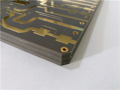
Wangling TP1020 Double-Sided 6.0mm PCB TP Series Substrates Low Moisture Absorption 0.01% for Global Satellite Navigation
Wangling TP1020 Double-Sided 6.0mm PCB TP Series Substrates Low Moisture Absorption 0.01% for Global Satellite Navigation
Printed Circuit Boards are custom-made products; the images and specifications provided are for reference only.
1.Introduction of TP series
TP material stands out as a one-of-a-kind high-frequency thermoplastic in the industry, with TP-type laminates featuring a dielectric layer composed of ceramics and polyphenylene oxide (PPO) resin—no fiberglass reinforcement included, a design that sets it apart for precision high-frequency applications. A key strength of TP material lies in its ability to tailor dielectric constant (Dk) with precision: by adjusting the ratio of ceramics to PPO resin, manufacturers can fine-tune Dk to meet exact circuit needs, while its specialized production process ensures exceptional dielectric performance and long-term reliability across all TP variants. Importantly, the TP lineup is categorized by copper-clad configurations to match diverse PCB assembly demands: TP refers to copper-free laminates with a smooth surface, ideal for custom post-processing; TP-1 denotes single-sided copper-clad laminates, and TP-2 is engineered for double-sided copper cladding—all built to maintain the core dielectric advantages of TP material.
What makes TP material even more versatile for PCB designs is its broad, stable Dk range: it can be selected arbitrarily from 3.0 to 25.0, with consistent performance that doesn’t fluctuate unexpectedly in real-world use. Common Dk options align with specific TP models to simplify sourcing, including 3.0 (TP300), 4.4 (TP440), 6.0 (TP600), 6.15 (TP615), 9.2 (TP920), 9.6 (TP960), 9.8 (TP980), 10.2 (TP1020), 11.0 (TP1100), 16.0 (TP1600), and 20.0 (TP2000)—each model optimized to deliver the exact Dk required for applications like satellite navigation or miniaturized antennas. Complementing this Dk flexibility is TP material’s ultra-low dielectric loss: while loss does increase marginally as frequency rises, the change remains insignificant within the 10 GHz range—a critical trait for high-frequency PCBs where signal integrity is non-negotiable. This low-loss, stable performance is consistent across the entire TP series, from entry-level TP300 to high-Dk TP2000, making TP material a go-to choice for engineers designing reliable, high-performance PCBs.
2. Features of TP1020 PCB
- Dielectric constant (Dk) of 10.2±0.2 at 10GHz
- Dissipation factor of .0012 at 10GHz
- Low TCDK at -40 ppm/°C, -55°C to 150°C
- CTE x-axis of 40 ppm/°C, CTE y-axis of 40 ppm/°C, CTE z-axis of 55 ppm/°C, -55°C to 150°C
- Thermal conductivity of 0.67 W/mk
- Moisture absorption of 0.01%
- UL 94-V0
3. PCB Stackup:
2-layer rigid PCB
Copper_layer_1 - 35 μm
TP1020 Core - 5.93 mm (233.5mil)
Copper_layer_2 - 35 μm
4. PCB Construction Details:
- Base material: TP1020
- Layer count: Double sided
- Board dimensions: 129mm x 129 mm=1PCS, +/- 0.15mm
- Minimum Trace/Space: 5/8 mils
- Minimum Hole Size: 0.7mm
- No Blind vias.
- Finished board thickness: 6.0mm
- Finished Cu weight: 1oz (1.4 mils) inner layer / outer layers
- Via plating thickness: 20 μm
- Surface finish: Electroless Nickel Immersion Gold (ENIG)
- Top Silkscreen: NO
- Bottom Silkscreen: No
- Top Solder Mask: NO
- Bottom Solder Mask: No
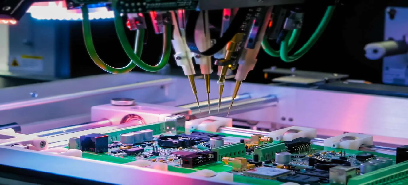
- 100% Electrical test used prior to shipment
5. PCB Statistics:
Components: 19
Total Pads: 70
Thru Hole Pads: 42
Top SMT Pads: 28
Bottom SMT Pads: 0
Vias: 37
Nets: 2
6. Type of artwork supplied:
Gerber RS-274-X
7. Quality standard:
IPC-Class-2
8. Availability:
Worldwide
9. Typical Applications:
- Global Satellite Navigation System
- missile-borne
- fuze technology
- miniaturized antenna