

 Home
-
Newly shipped PCBs
-
Rogers RO4360G2 PCB: 0.9mm Dual-Layer High-Dk Thermoset Board for Telecommunications Infrastructure
Home
-
Newly shipped PCBs
-
Rogers RO4360G2 PCB: 0.9mm Dual-Layer High-Dk Thermoset Board for Telecommunications Infrastructure
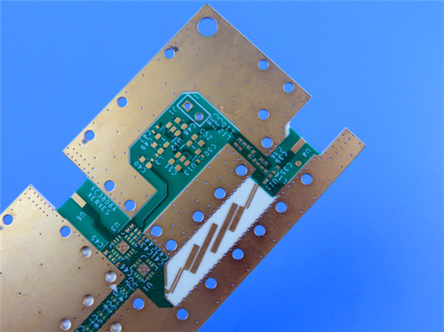
Rogers RO4360G2 PCB: 0.9mm Dual-Layer High-Dk Thermoset Board for Telecommunications Infrastructure
Printed Circuit Boards are custom-made products; the images and specifications provided are for reference only.
1.Rogers RO4360G2 PCB Introduction
Rogers RO4360G2 PCB utilizes innovative low-loss, glass-reinforced hydrocarbon ceramic thermoset materials that deliver an optimal balance between high-frequency performance and manufacturing efficiency. This 2-layer 0.9mm thick circuit board represents a breakthrough as the first high dielectric constant thermoset laminate compatible with standard FR-4 processing methods. Rogers RO4360G2 material's enhanced rigidity improves handling in multi-layer constructions while reducing both material and fabrication expenses, offering seamless integration with RO440 series prepregs and other RO4000 laminates in complex multi-layer designs.
2.Material Features
Dielectric Constant: 6.15 ±0.15 at 10 GHz/23°C
Dissipation Factor: 0.0038 at 10 GHz/23°C
Thermal Decomposition Temperature: >407°C
Glass Transition Temperature: >280°C (TMA method)
Thermal Conductivity: 0.75 W/m·K
Z-axis CTE: 28 ppm/°C
X-Y Axis CTE: X axis 13 ppm/°C, Y axis 14 ppm/°C (-55 to 288°C)
Lead-Free Process Compatible
Flammability Rating: 94V-0
3.Material Benefits
Enhanced Design Flexibility for Complex Circuit Layouts
Superior Plated Through-Hole Reliability
Full Compatibility with Automated Assembly Processes
Environmentally Friendly Lead-Free Manufacturing
Efficient Supply Chain with Reduced Lead Times
Cost-Effective Material Solution
Excellent Multi-layer Board Processability
Improved Rigidity for Enhanced Handling
4.PCB Construction Details
Base Material: RO4360G2
Layer Count: 2 Layers
Board Dimensions: 73.12mm x 44.71mm (1 PC)
Minimum Trace/Space: 5/6 mils
Minimum Hole Size: 0.30mm
Blind Vias: None
Finished Board Thickness: 0.9mm
Finished Copper Weight: 1 oz outer layers
Via Plating Thickness: 20 μm
Surface Finish: Immersion Gold
Top Silkscreen: White
Bottom Silkscreen: No
Top Solder Mask: Green
Bottom Solder Mask: No
Electrical Test: 100% Tested Prior to Shipment
5.PCB Stackup: 2-Layer Rigid Construction
Copper Layer 1: 35 μm
Rogers RO4360G2 Substrate: 32mil (0.813mm)
Copper Layer 2: 35 μm
6.PCB Assembly Statistics
Components: 16
Total Pads: 53
Thru Hole Pads: 37
Top SMT Pads: 16
Bottom SMT Pads: 0
Vias: 49
Nets: 2
7.Artwork and Quality Standards
Artwork Format: Gerber RS-274-X
Accepted Standard: IPC-Class-2
Availability: Worldwide
8.Typical Applications
Base Station Power Amplifiers
Small Cell Transceivers
Wireless Infrastructure Equipment
Telecommunications Hardware
RF Communication Systems
9.Conclusion
Rogers RO4360G2 PCB provides a sophisticated high-Dk thermoset solution that combines advanced electrical properties with practical manufacturing advantages, delivering reliable performance for modern telecommunications infrastructure and wireless communication systems.