

 Home
Home
How to Avoid Common PCB Pitfalls: 7 Design Principles You Need to Know
PCB design is a foundational phase in electronics development, critically influencing circuit performance, manufacturing cost, and end-product reliability. This article outlines seven essential principles to help engineers achieve robust, efficient, and production-ready board designs.
1.Standardized Schematic Design
A well-organized schematic is the cornerstone of a successful PCB. Adopt a modular design approach, grouping circuits functionally across sheets. Annotate design constraints and layout notes directly in the schematic to streamline collaboration and reduce errors. Reusing validated circuit blocks accelerates development and minimizes risk.
2.Strategic Component Placement
Layout planning directly impacts signal integrity and EMI performance. Follow natural signal flow paths and group related circuits together. Isolate analog and digital sections, partition power supplies from sensitive signals, and keep noise-sensitive components away from heat sources. A logical placement simplifies routing and improves performance.
3.Comprehensive Design Rule Configuration
Leverage modern EDA tools to enforce design rules automatically. Define constraints for trace width, clearances, matched lengths, and via usage. Pay special attention to power and ground nets to ensure low-impedance return paths. Consistent rule application reduces manual errors and ensures design reproducibility.
4.Controlled Impedance and High-Speed Routing
For high-frequency signals (>200MHz), adopt impedance-controlled routing and consider multilayer stack-ups. Use curved traces instead of right-angle turns to minimize reflections. In two-layer designs, apply orthogonal routing between layers to reduce crosstalk. Above 350MHz, select specialized high-frequency laminates to maintain signal integrity.
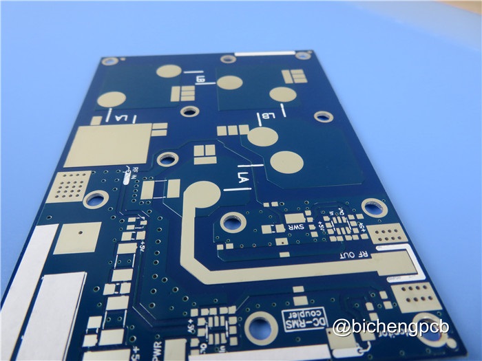
RF-45 PCB with Blue Solder Mask Coating Immersion Silver
5.Design for Manufacturing (DFM) and Test (DFT)
Optimize layouts for manufacturability: maintain consistent part orientation, provide adequate clearance for tooling, and include fiducials and breakaway tabs. For prototypes, add test points and descriptive silkscreen to simplify validation. Incorporating DFM/DFT early significantly reduces respins and field failures.
6.Rigorous Verification and Attention to Detail
Thoroughly verify component footprints and pin assignments before release. Implement a checklist-based review process for layout and output files. Small oversights in packaging or connectivity can lead to costly rework. Diligence in final verification is crucial for error-free fabrication.
7.Simulation-Driven Design Refinement
Use SI/PI simulations to evaluate signal quality, power delivery, and EMI behavior before prototyping. Start with critical nets and power systems to identify potential issues early. While simulation models are not perfect, they provide invaluable insight and help avoid major redesigns.
8.Conclusion
Excellent PCB design requires methodical planning, adherence to established high-speed design practices, and meticulous verification. By integrating these seven principles into your workflow, you can create high-performance, reliable, and manufacturable circuit boards that meet both electrical and mechanical requirements. Investing in good design habits ultimately shortens development cycles and boosts product quality.
PCB Design Core Process Table
Process Stages |
Key Ops |
Objectives |
1. Design Initiation & Requirements |
Clarify functions/performance; distinguish mass-produced/dev boards |
Define scope; avoid deviations |
2. Standardized Schematic |
Module-based schematics (page-split); mark layout notes; reuse mature circuits |
Lay foundation; boost collaboration; ease debugging |
3. Scientific Layout |
Layout by signal flow; separate analog/digital/power; keep sensitive parts away from heat; reserve high-frequency shielding |
Optimize SI/EMC; save routing time |
4. Design Rule Setting |
Set trace width/spacing/equal-length; optimize power/ground low-impedance paths |
Avoid human errors; ensure consistency |
5. Professional Routing |
Routine routing (ordinary circuits); high-frequency: multi-layer/special materials, arc/orthogonal routing |
Control impedance; reduce crosstalk |
6. Design for Mfg & Usability |
Mass production: unify component orientation + process edges; Dev boards: silk screen + test points |
Balance needs; cut support workload |
7. Detailed Quality Control |
Verify component package/pins (vs. physical parts); conduct design inspection |
Avoid scrapping (low-level errors); ensure reliability |
8. Simulation & Fabrication |
Run SI/PI simulations; adjust layout/routing if failed; confirm before fabrication |
Identify issues early; optimize design; meet standards |