


 Home
-
F4B PCB
-
F4BTM300 2-Layer High Frequency PCB Built on 20mil Laminate with Immersion Gold for Radar and Feed Networks
F4BTM300 2-Layer High Frequency PCB Built on 20mil Laminate with Immersion Gold for Radar and Feed Networks
Printed Circuit Boards are custom-made products; the images and specifications provided are for reference only.
1. Product Overview of F4BTM300 2-Layer PCB
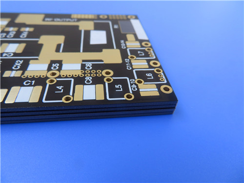
F4BTM300 2-Layer PCB is a custom rigid high frequency PCB fabricated from F4BTM300 ceramic-filled PTFE copper clad laminate. This PCB comes with 0.6mm finished board thickness and 1oz finished copper weight on outer layers, and it adopts differentiated solder mask and silkscreen construction. The top layer features black solder mask with white silkscreen, while the bottom layer is manufactured with no solder mask and no silkscreen. Immersion gold is selected as the surface finish, which improves solderability, oxidation resistance and electrical conductivity for stable long-term operation. The finished dimension of this PCB is 105.4mm × 76mm per piece with dimensional tolerance +/- 0.15mm. Every unit undergoes 100% electrical test before shipment to guarantee circuit integrity and reliability.
As a high-performance ceramic-filled PTFE circuit board, F4BTM300 2-Layer PCB is designed for high-speed signal transmission, microwave and RF applications including aerospace, radar and satellite communication. It retains the low dielectric loss, stable dielectric constant and low thermal expansion properties of F4BTM300 substrate to reduce signal attenuation and frequency drift under high frequency conditions. The symmetrical stackup design balances mechanical and electrical performance, making it a reliable option for military-grade and aerospace wireless communication projects.
2. F4BTM300 PCB Core Specification Parameters
| Parameter Item | Specification Details |
| Base Material | F4BTM300 Ceramic-Filled PTFE Copper Clad Laminate |
| Layer Count | 2-Layer Rigid PCB |
| Finished Board Thickness | 0.6mm |
| Finished Copper Weight (Outer Layers) | 1oz (1.4 mils) |
| Via Plating Thickness | 20 μm |
| Minimum Trace / Space | 5/8 mils |
| Minimum Hole Size | 0.35mm |
| Blind Vias | No Blind Vias |
| Top Layer Treatment | Black Solder Mask, White Silkscreen |
| Bottom Layer Treatment | No Solder Mask, No Silkscreen |
| Surface Finishing | Immersion Gold |
| Product Dimension | 105.4mm × 76mm, Tolerance +/- 0.15mm |
| Artwork Format | Gerber RS-274-X |
| Quality Standard | IPC-Class-2 |
| Electrical Test | 100% Electrical Test Prior to Shipment |
| Availability | Worldwide |
3. PCB Stackup Structure
F4BTM300 2-layer rigid PCB adopts standard symmetrical stackup design to guarantee consistent electrical performance and mechanical stability:
- Copper_layer_1 – 35 μm
- F4BTM300 Core – 0.508 mm (20mil)
- Copper_layer_2 – 35 μm
4. PCB Statistics
F4BTM300 double- layer PCB includes 13 components with a total of 94 pads, consisting of 51 thru hole pads and 43 top SMT pads. There are 0 bottom SMT pads, 36 vias and 2 nets on the circuit.
5. F4BTM300, F4BTM and F4BTME Series Copper Clad Laminate Material Knowledge
5.1 Material Overview
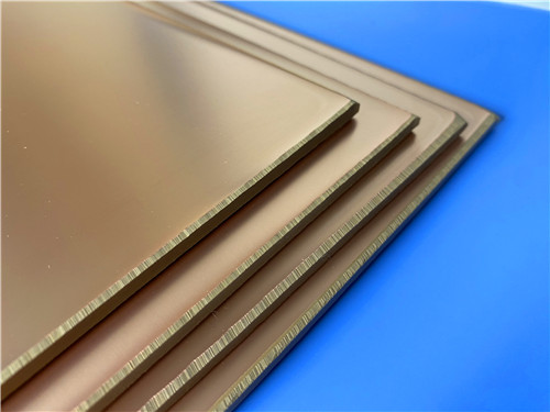
F4BTM300 belongs to the F4BTM series, while F4BTM series and F4BTME series are two independent lines of ceramic-filled PTFE fiberglass cloth copper-clad laminates, specially developed for high frequency, microwave and aerospace PCB fabrication. These substrates are manufactured through a meticulous process blending fiberglass cloth, nano-ceramic fillers, and PTFE resin, built upon the mature F4BM dielectric foundation. Nano-ceramic filler doping delivers higher dielectric constant, improved heat resistance, lower thermal expansion coefficient, higher insulation resistance and better thermal conductivity while preserving low dielectric loss. Though they share the same ceramic-filled PTFE dielectric layer, F4BTM series and F4BTME series are separate product lines defined by different copper foil selections and PIM performance targets.
F4BTM series uses ED electrodeposited copper foil, suited for general RF and microwave projects without strict PIM requirements. F4BTM300 is a core specialized grade inside the F4BTM series with fixed Dk 3 +/-0.06 at 10GHz for precise high-frequency design applications. F4BTME series adopts reverse-treated RTF copper foil to achieve superior PIM performance, tighter impedance control and lower conductor loss, which serves high-precision passive RF circuits, radar and base station applications.
The F4BTM family supports customizable dielectric constant ranging from 2.98 to 3.5. Formulation tuning balances low signal attenuation and good dimensional stability. The series features rich core thickness options and multiple standard substrate sizes to improve material utilization and reduce overall production cost. All grades support mass commercial production and feature radiation resistance plus ultra-low outgassing for harsh environment deployment.
5.2 Core Material Features of F4BTM300
- Dielectric constant (Dk) of 3 +/-0.06 at 10GHz
- Dissipation factor of 0.0018 at 10GHz, 0.0023 at 20GHz
- CTE x-axis of 15 ppm/°C, CTE y-axis of 16 ppm/°C, CTE z-axis of 78 ppm/°C, ranging -55°C to 288°C
- Low thermal coefficient of Dk at -75 ppm/°C, ranging -55°C to 150°C
- PIM value < -160 dbc
- Moisture absorption of 0.05%
5.3 Typical Application Scenarios
F4BTM300, F4BTM and F4BTME ceramic-filled PTFE copper-clad laminates are widely adopted in high-frequency, microwave, RF and aerospace electronic industries, covering the following mainstream applications:
- Aerospace equipment, space and cabin equipment
- Microwave and RF devices
- Radar and military radar systems
- Antenna feed networks
- Phase-sensitive antennas and phased array antennas
- Satellite communication equipment
6. Datasheet
| Product Model/Data | Property | Test Condition | Unit | F4BTM300 | |
| F4BTM300 | Dielectric Constant (Typical Value) | 10GHz | - | 3.0 | |
| F4BTM300 | Dielectric Constant Tolerance | - | - | ±0.06 | |
| F4BTM300 | Dissipation Factor (Typical Value) | 10GHz | - | 0.0018 | |
| F4BTM300 | Dissipation Factor (Typical Value) | 20GHz | - | 0.0023 | |
| F4BTM300 | Temperature Coefficient of Dielectric Constant | -55℃~150℃ | ppm/℃ | -75 | |
| F4BTM300 | Peel Strength | 1 OZ F4BTM | N/mm | >1.6 | |
| F4BTM300 | Peel Strength | 1 OZ F4BTME | N/mm | >1.4 | |
| F4BTM300 | Volume Resistivity | Normal Condition | MΩ.cm | ≥1×10⁷ | |
| F4BTM300 | Surface Resistance | Normal Condition | MΩ | ≥1×10⁶ | |
| F4BTM300 | Electric Strength (Z Direction) | 5KW, 500V/s | KV/mm | >30 | |
| F4BTM300 | Breakdown Voltage (XY Direction) | 5KW, 500V/s | KV | >35 | |
| F4BTM300 | Coefficient of Thermal Expansion (XY Direction) | -55℃~288℃ | ppm/℃ | 15, 16 | |
| F4BTM300 | Coefficient of Thermal Expansion (Z Direction) | -55℃~288℃ | ppm/℃ | 72 | |
| F4BTM300 | Thermal Stress | 260℃, 10s, 3 cycles | - | No Delamination | |
| F4BTM300 | Water Absorption | 20±2℃, 24h | % | ≤0.05 | |
| F4BTM300 | Density | Ambient Temperature | g/cm³ | 2.25 | |
| F4BTM300 | Continuous Operating Temperature | Thermal Chamber | ℃ | -55~+260 | |
| F4BTM300 | Thermal Conductivity (Z Direction) | - | W/(M.K) | 0.42 | |
| F4BTM300 | PIM Value | Only for F4BTME | dBc | ≤-160 | |
| F4BTM300 | Flammability | - | UL-94 | V-0 | |
| F4BTM300 | Material Composition | - | - | PTFE, Fiberglass ClothF4BTM matched with ED copper foil, F4BTME matched with reverse RTF copper foil |
7. Summary
F4BTM300 2-Layer 0.6mm high frequency PCB is a high-performance circuit board customized based on ceramic-filled PTFE F4BTM300 copper clad laminate. With 1oz finished outer copper and immersion gold surface treatment, F4BTM300 rigid PCB features stable electrical conductivity, outstanding oxidation resistance and excellent solderability. The symmetrical stackup structure and differentiated solder mask / silkscreen design meet special assembly requirements for aerospace and radar systems. Adopting F4BTM300 ceramic-filled substrate material, F4BTM300 PCB inherits the advantages of low dielectric loss, tight Dk tolerance, low thermal expansion and low outgassing, which can fully meet the demanding working requirements of RF, microwave, radar and satellite communication equipment. Manufactured to IPC-Class-2 standards and 100% electrically tested before delivery, F4BTM300 laminate PCB is a reliable choice for commercial and aerospace high-frequency wireless communication applications.