

 Home
-
Antenna PCB
-
TP440 2-Layer 0.6mm High Frequency PCB with Immersion Gold Surface Finish for GPS and Miniature Antenna Applications
Home
-
Antenna PCB
-
TP440 2-Layer 0.6mm High Frequency PCB with Immersion Gold Surface Finish for GPS and Miniature Antenna Applications
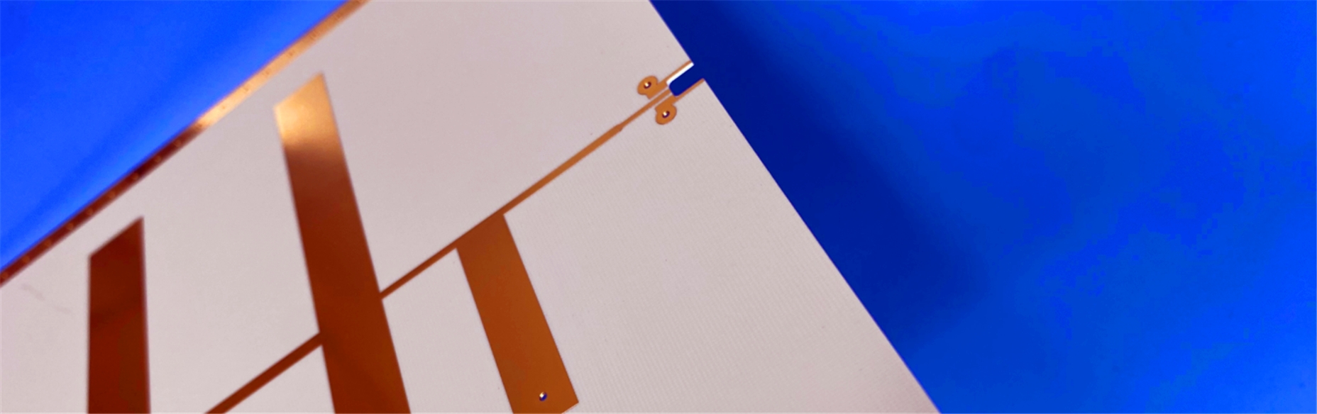
TP440 2-Layer 0.6mm High Frequency PCB with Immersion Gold Surface Finish for GPS and Miniature Antenna Applications
Printed Circuit Boards are custom-made products; the images and specifications provided are for reference only.
1. Introduction
Wangling TP440 PCB is a premium 2-layer rigid high frequency printed circuit board built on authentic 0.5mm TP440 laminate, designed for high-precision RF circuits and miniature antenna systems. TP440 0.6mm finished high frequency PCB adopts exclusive Wangling TP440 thermoplastic dielectric substrate, featuring ceramic and Polyphenylene Oxide (PPO) composite structure without fiberglass reinforcement. The TP440 core material supports precisely adjustable dielectric constant and delivers ultra-stable high-frequency performance under 10 GHz. Manufactured with specialized high-frequency substrate processing techniques, TP440 laminate PCB provides low dielectric loss, reliable copper foil adhesion and outstanding thermal stability. Finished with immersion gold surface treatment and certified to IPC-Class-2 standards, every TP440 high frequency PCB undergoes 100% electrical testing before shipment, ensuring stable performance and worldwide availability for military, aerospace and positioning antenna applications.
2. Core Features
TP440 high frequency PCB inherits all superior properties of original TP440 thermoplastic copper clad laminate substrate. First, the TP440 material supports customizable dielectric constant ranging from 3 to 25, covering widely used values 3.0, 4.4, 6.0, 6.15, 9.2, 9.6, 10.2, 11, 16 and 20, maintaining highly stable dielectric performance at high frequencies. The TP440 PCB features ultra-low dielectric loss, with only minor loss fluctuation within 10 GHz frequency band. Second, the TP440-based PCB achieves a wide long-term operating temperature range of -100°C to +150°C, delivering excellent low-temperature resistance for extreme environment deployment. Temperatures above 180°C may cause TP440 substrate deformation, copper foil peeling and electrical performance deviation. Third, the 0.5mm TP440 core supports ultra-thin PCB design, with a finished board thickness of 0.6mm, and allows multiple thickness customization options. Fourth, TP440 substrate offers strong radiation resistance and low outgassing performance, suitable for aerospace-grade equipment. Fifth, TP440 PCB is the ideal circuit board solution for Beidou systems, missile-borne devices, fuze modules and compact miniaturized antennas. Sixth, the TP440 dielectric layer provides stronger copper foil adhesion compared with traditional ceramic substrates, allowing flexible mechanical processing including drilling, grinding, turning and etching, which greatly improves PCB manufacturability.
3. Product Benefits
Adopting genuine 0.5mm Wangling TP440 core material, this 2-layer high frequency PCB brings significant technical and commercial advantages for high-frequency electronic products. The highly stable dielectric property of TP440 material minimizes high-frequency signal loss, ensuring precise and consistent RF signal transmission for antenna and microwave circuits. The extreme low-temperature resistance and radiation resistance of TP440 substrate greatly enhance equipment reliability in military and aerospace harsh environments. The ultra-thin 0.5mm TP440 core structure enables lightweight and miniaturized product design, meeting the trend of compact electronic devices. Compared with ceramic substrate PCBs, TP440 copper clad laminate features superior bonding strength and machining flexibility, effectively improving production yield and reducing manufacturing costs. All Wangling TP440 high frequency PCBs comply with IPC-Class-2 quality standards and pass full electrical testing, delivering consistent, reliable and globally available high-frequency circuit board solutions.
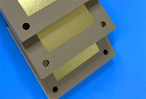
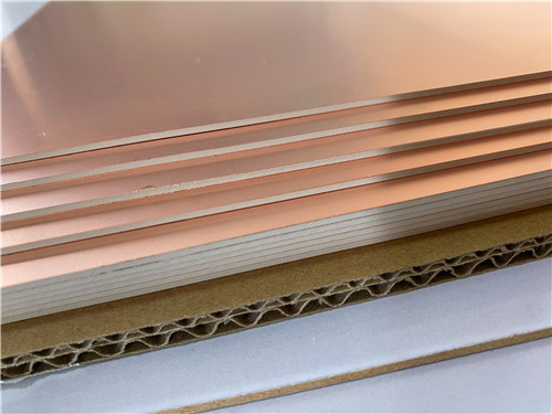
4. PCB Construction Details
Specification Item |
Detailed Parameters |
Board Dimensions |
67.5mm x 58.6mm (1PCS), Tolerance: +/- 0.15mm |
Minimum Trace/Space |
6/8 mils |
Minimum Hole Size |
0.3mm |
Blind Vias Design |
No Blind Vias |
Finished Board Thickness |
0.6mm |
Finished Copper Weight (Outer Layers) |
1oz (1.4 mils) |
Via Plating Thickness |
20 μm |
Surface Finish |
Immersion Gold |
Top Silkscreen |
No |
Bottom Silkscreen |
No |
Top Solder Mask |
No |
Bottom Solder Mask |
No |
Pre-Shipment Testing |
100% Electrical Test |
5. PCB Stackup Structure
This TP440 2-layer laminate PCB is a rigid circuit board built with genuine 0.5mm TP440 high-frequency core material, featuring a stable and professional stackup design optimized for RF signal performance:
1. Copper_layer_1: 35 μm
2. TP440 Core: 0.5 mm
3. Copper_layer_2: 35 μm
6. PCB Statistical Parameters
The complete component and circuit statistics of the finished Wangling TP high frequency PCB are shown below:
Components: 11
Total Pads: 19
Thru Hole Pads: 10
Top SMT Pads: 9
Bottom SMT Pads: 0
Vias: 7
Nets: 1
7. Artwork Supply Type
The PCB design artwork is provided in standard Gerber RS-274-X format, which is universally compatible with global PCB manufacturing and processing equipment, ensuring accurate pattern reproduction and consistent production quality.
8. Quality Standard
Wangling TP high frequency PCB strictly complies with IPC-Class-2 industry quality standards, meeting the reliability and stability requirements of commercial and industrial high-frequency electronic equipment.
9. Product Availability
TP series of high frequency PCB supports worldwide supply and distribution, providing stable and reliable product supply for global electronic manufacturers and engineering projects.
10. Wangling TP Material Introduction
TP PCB material is a specialized high-frequency thermoplastic material widely used in the high-end PCB industry. Different from traditional PCB substrates, the dielectric layer of TP-type laminates is composed of ceramic and Polyphenylene Oxide (PPO) resin without fiberglass reinforcement. The dielectric constant of the material can be precisely adjusted by modifying the mixing ratio of ceramic powder and PPO resin. With unique customized production technology, Wangling TP material delivers excellent high-frequency dielectric performance and long-term working reliability. In material classification, TP represents smooth non-copper-clad substrate, TP-1 stands for single-sided copper-clad material, and TP-2 refers to double-sided copper-clad substrate, covering diverse PCB design and manufacturing needs.
11. Typical Applications
With superior high-frequency performance and extreme environmental adaptability, the Wangling TP 2-layer high frequency PCB is widely applied in high-precision and special scenario equipment, including GPS antenna equipment, missile-borne electronic systems, fuze devices, and various miniaturized antenna products.
12. TP Copper Clad Laminate Knowledge
Wangling TP CCL is a unique high-frequency thermoplastic copper clad laminate exclusive in the PCB substrate industry. Different from conventional glass fiber-reinforced PCB materials, the dielectric layer of the TP-series CCL is composed of ceramic and Polyphenylene Oxide (PPO) resin with no fiberglass reinforcement. Its dielectric constant can be precisely and flexibly adjusted by modifying the proportion of ceramic filler and PPO resin. Adopting exclusive and specialized production craftsmanship, this TP CCL substrate delivers outstanding dielectric stability, low signal loss and long-term working reliability for high frequency PCB manufacturing. In terms of material classification, TP refers to non-copper-clad smooth substrate, TP-1 represents single-sided copper-clad-laminate, and TP-2 stands for double-sided copper clad laminate, covering diverse single and double-layer high frequency PCB production demands.
Stable and Customizable Dielectric Properties: The dielectric constant of Wangling TP copper clad laminate can be arbitrarily customized within 3 to 25 according to actual high-frequency circuit design requirements. Common mainstream dielectric constant specifications include 3.0, 4.4, 6.0, 6.15, 9.2, 9.6, 10.2, 11, 16 and 20. The substrate features ultra-low dielectric loss; although loss rises slightly with frequency increase, the electrical performance remains stable with negligible changes within 10 GHz, making it ideal for high-frequency signal transmission PCBs.
Superior Wide Temperature Resistance: This TP substrate supports long-term stable operation at temperatures ranging from -100°C to +150°C, possessing excellent low-temperature resistance suitable for extreme environment applications. When the ambient temperature exceeds 180°C, the substrate may suffer deformation, copper foil peeling and obvious attenuation of electrical performance, so high-temperature working scenarios above 180°C should be avoided.
Diversified Customizable Thickness: The minimum thickness of Wangling TP base material is 0.5mm, with a complete range of conventional thickness specifications. It supports personalized thickness customization to meet the design requirements of ultra-thin miniaturized high frequency PCBs.
Excellent Environmental Adaptability: The TP substrate boasts reliable radiation resistance and low outgassing performance, adapting to harsh working environments of aerospace and military electronic equipment.
Professional Application Orientation: As a high-performance high-frequency substrate, Wangling TP CCL is the optimal core material for manufacturing Beidou positioning equipment, missile-borne electronic devices, fuze modules and various miniaturized antenna PCBs.
Superior Machining and Adhesion Performance: The bonding force between copper foil and dielectric layer of TP laminate is far more stable and reliable than vacuum-coated ceramic substrates. The thermoplastic substrate supports multiple mechanical processing methods including drilling, turning, grinding, shearing and etching, which cannot be realized by traditional ceramic substrates, greatly improving processing flexibility.
High Yield and Low Processing Cost: Wangling TP copper clad laminate can be processed by standard thermoplastic material manufacturing processes, featuring high finished product yield and significantly lower production costs compared with expensive ceramic substrates. Considering its material properties, multi-layer PCB fabrication is not recommended. If multi-layer processing is required, low-temperature bonding sheets must be adopted with full feasibility verification in advance.
Standard Welding Processing Specifications: This TP PCB substrate cannot withstand 260°C thermal shock and is not applicable for wave soldering processes. Constant-temperature manual soldering with an electric iron is the recommended processing method. Reflow soldering is generally not advised; if reflow soldering is necessary, the maximum temperature setting shall not exceed 200°C, and sufficient verification of processing feasibility and product stability is required.
13. Product Summary
Wangling 2-layer TP440 high frequency PCB is a high-performance ultra-thin rigid circuit board built on 0.5mm TP440 core copper clad laminate, tailored for miniature antenna and military high-frequency electronic systems. With customizable stable dielectric constant, ultra-low 10 GHz band loss, excellent low-temperature resistance and superior machinability, this 0.6mm immersion gold TP440 PCB meets IPC-Class-2 quality standards. It effectively overcomes the defects of poor stability and high processing cost of traditional ceramic substrates, providing reliable core PCB solutions for GPS, Beidou, missile-borne and fuze miniaturized antenna equipment with stable global supply capacity.
14. TP440 Datasheet
| Property | Test Condition | Unit | TP440 |
| Dielectric Constant | 10 GHz | / | 4.4 ± 0.09 |
| Dielectric Constant Tolerance | / | / | ±2% |
| Dissipation Factor | 10 GHz | / | 0.0010 |
| Temperature Coefficient of Dielectric Constant | -55℃ ~ 150℃ | ppm/℃ | -50 |
| Peel Strength (1 OZ, Normal Condition) | 1 OZ, Normal Condition | N/mm | >0.6 |
| Peel Strength (1 OZ, After Alternating Humid Heat) | 1 OZ, After Alternating Humid Heat | N/mm | >0.4 |
| Volume Resistivity (500V, Normal Temperature) | 500V, Normal Temperature | MΩ·cm | >1×10⁹ |
| Surface Resistivity (500V, Normal Temperature) | 500V, Normal Temperature | MΩ | >1×10⁷ |
| Coefficient of Thermal Expansion (X, Y, Z axis) | -55℃ ~ 150℃ | ppm/℃ | 60, 60, 70 |
| Water Absorption | 20±2℃, 24 h | % | ≤0.01 |
| Continuous Operating Temperature | Temperature Chamber | ℃ | -100℃ ~ 150℃ |
| Density | / | g/cm³ | 1.89 |
| Thermal Conductivity | / | W/(m·K) | 0.44 |
| Material Composition | / | / | Polyphenylene Ether, Ceramic; Matched with ED Copper Foil |