


 Home
-
Hybrid PCB
-
Rogers RO4350B 8-Layer Palladium Gold PCB 0.168Mm RO4350B and 0.381Mm MT40 and 0.1245Mm MT40 Prepreg PCB For RF Module
Rogers RO4350B 8-Layer Palladium Gold PCB 0.168Mm RO4350B and 0.381Mm MT40 and 0.1245Mm MT40 Prepreg PCB For RF Module
Printed Circuit Boards are custom-made products; the images and specifications provided are for reference only.
1. Introduction
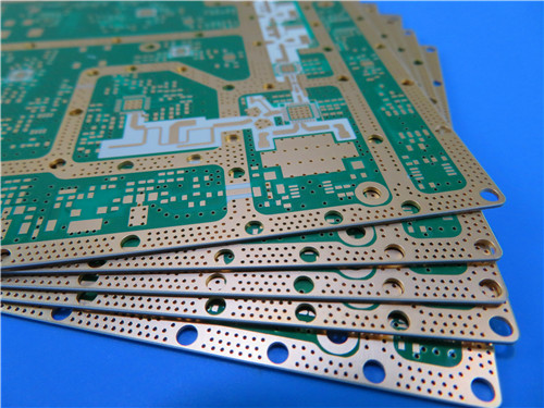
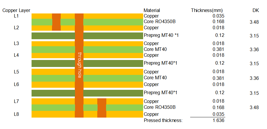
8-layer hybrid dielectric Rogers RO4350B PCB is a multilayer RF printed circuit board built with dual-side 0.168mm RO4350B high frequency laminate, middle 0.381mm I-Tera MT40 substrate and 0.1245mm MT40 prepreg. This RO4350B PCB adopts mixed dielectric stackup design, retaining premium RF performance on top and bottom signal layers while using cost-effective MT40 material for inner layers. The finished laminated thickness of this 8-layer RO4350B PCB reaches 1.636mm, with 1oz finished outer copper and 0.5oz finished inner copper. The board uses green solder mask with white silkscreen and palladium gold surface finish. It is designed with L1-L2 and L7-L8 blind vias, and 6mil single-ended traces on the top layer for 50-ohm impedance control, perfectly suited for medium and large size RF module projects. Special manufacturing considerations derived from the official I-Tera MT40 processing guide must be followed to guarantee reliability for this RO4350B hybrid PCB.
2. Features
- Top and bottom 0.168mm RO4350B laminates deliver low Df and low dielectric loss to minimize microwave signal attenuation
- Top layer 6mil trace is engineered for 50-ohm single-ended impedance to satisfy RF signal transmission requirements
- Middle 0.381mm I-Tera MT40 high Tg substrate provides solid mechanical support and outstanding thermal stability
- 0.1245mm MT40 prepreg precisely controls interlayer dielectric thickness and stabilizes total board thickness at 1.636mm
- I-Tera MT40 material has stable Dk from -55°C to +125°C up to W-band frequencies, Dk=3.45, Df=0.0031, Tg 215°C, Td 360°C
- Blind via structure: L1-L2, L7-L8
- Green solder mask, white silkscreen and palladium gold surface finish
- 1oz outer copper weight, 0.5oz inner copper weight
- 100% Electrical test before shipment and compliant with IPC-Class-2 quality standard
- I-Tera MT40 follows FR-4-compatible workflow with defined prepreg storage, lamination, drilling and desmear requirements per official processing guide
3. Benefits
- This 8-layer RO4350B hybrid PCB adopts RO4350B on both outer signal layers and I-Tera MT40 for inner layers. The outer RO4350B reduces microwave signal loss, while inner MT40 ensures mechanical strength and thermal performance, cutting material cost significantly compared with full RO4350B stackup.
- I-Tera MT40 supports multiple SMT reflow cycles and multi-time lamination processes, improving thermal reliability of the RO4350B hybrid PCB and avoiding the thermal drawbacks of full ceramic high-frequency boards.
- The mixed dielectric stackup only uses high-frequency RO4350B on signal layers, and applies economical MT40 for power and ground layers, optimizing material utilization for mass production of medium and large RF modules.
- RO4350B and MT40 have different CTE values. Segmented gradient heating and slow cooling lamination process is implemented to prevent interlayer delamination and board warpage. Extra registration targets and uniform pressure control on lamination plates are added to reduce layer shift risks for this 8-layer thick PCB.
- Dielectric thickness fluctuation directly affects impedance performance. Strict raw material thickness tolerance inspection is required to guarantee stable 50-ohm single-ended impedance for the 6mil top traces of this RO4350B PCB.
- Following I-Tera MT40 official processing guidelines minimizes dimensional shift, hole-wall defects and delamination risks for RO4350B + MT40 hybrid PCB mass production.
4. PCB Construction details
| Item | Specification |
| Base material | 0.168mm RO4350B + 0.381mm I-Tera MT40 + 0.1245mm MT40 Prepreg |
| Layer count | 8-Layer rigid hybrid dielectric PCB |
| Board dimensions | 179 mm x 121 mm=1PCS |
| Finished laminated thickness | 1.636mm |
| Inner copper weight | 0.5oz |
| Finished outer Cu weight | 1oz outer layers |
| Blind Via | L1-L2, L7-L8 blind vias |
| Top Trace Specification | 6mil trace, 50 Ohm single-ended impedance |
| Surface finish | Palladium gold |
| Top Silkscreen | White |
| Bottom Silkscreen | White |
| Top Solder Mask | Green |
| Bottom Solder Mask | Green |
| Pre-shipment test | 100% Electrical test used prior to shipment |
5. PCB Stackup: 8-layer hybrid rigid PCB
6.Type of artwork supplied: Gerber RS-274-X
7.Quality standard: IPC-Class-2
8. Availability: Worldwide
9. Some Typical Applications
- Radio frequency communication modules
- High-speed signal processing equipment
- Wireless transceiver hardware
- Broadband signal transmission devices
- Industrial wireless sensing modules
- High reliability signal control units
10. Rogers RO4350B & I-Tera MT40 Copper Clad Laminate Knowledge
I-Tera MT40 laminate and prepreg are designed for high speed digital and RF/microwave printed circuit designs. I-Tera MT40 provides stable dielectric constant Dk=3.45 across temperature range from -55°C to +125°C up to W-band frequencies, with low dissipation factor Df=0.0031. It serves as a cost-effective alternative to PTFE and other microwave & high-speed digital laminate materials.
10.1 I-Tera® MT40 Features
- Tg: 215°C, Td: 360°C, excellent thermal performance for lead-free assembly
- RoHS compliant, CAF resistant, fully compatible with standard FR-4 fabrication workflow
- Supports multiple reflow cycles and multiple lamination cycles
- No special through-hole treatment required compared with PTFE-based substrates
- Available in laminate and prepreg form with various copper foil types and copper weights
- Production bases available in Asia, North America and Europe for global supply
10.2 Stackup Design & Rationality Analysis
The dual-side RO4350B plus middle MT40 stackup delivers well-designed high-frequency performance for this 8-layer RO4350B hybrid PCB. The top and bottom 0.168mm RO4350B high-frequency laminates feature low Df and low dielectric loss, meeting the 50-ohm single-ended RF trace requirement on the top layer and reducing microwave signal attenuation. The middle 0.381mm MT40 high Tg substrate provides structural support and thermal stability, greatly cutting production cost compared with full ceramic high-frequency PCB. The 0.1245mm MT40 prepreg precisely adjusts interlayer thickness and locks the total laminated thickness at 1.636mm with controllable thickness tolerance.
Manufacturing teams must handle the CTE mismatch between RO4350B ceramic substrate and MT40 FR4 material. Segmented gradient heating and slow cooling process is adopted to reduce delamination and board warpage risks. For this 8-layer thick hybrid PCB, layer shift is a common defect. Adding alignment targets and optimizing pressure uniformity of lamination plates can effectively improve layer registration accuracy. Impedance performance is sensitive to dielectric thickness variation for alternating thin and thick dielectric stackup, so raw material thickness tolerance must be strictly controlled.
Replacing inner layers with economical MT40 brings obvious cost advantages to this 8-layer RO4350B hybrid PCB. The material cost is reduced, making it suitable for mass production of medium and large RF modules. MT40’s outstanding heat resistance withstands repeated SMT reflow soldering and compensates thermal reliability weakness of pure ceramic substrates. This stackup only reserves high-frequency RO4350B for outer signal layers, while inner power and ground layers adopt conventional FR4 material, maximizing material utilization efficiency.
10.3 Processing & Fabrication Notes (I-Tera MT40 Processing Guide)
Prepreg Storage & Handling: I-Tera MT40 prepreg shall be stored ≤23°C and below 50% RH. Allow temperature equilibration before opening packaging; do NOT vacuum-seal leftover MT40 prepreg after opening. Use FIFO inventory principle to avoid moisture-induced Tg depression and bad resin flowIsola Grou
Inner-layer Dimensional Control: Stress-relief bake is ineffective for I-Tera MT40. Characterize shrinkage of unbaked laminate and apply artwork compensation factors; most material movement occurs along the laminate grain direction
Lamination Parameters Reference: Follow MT40 recommended lamination profile: cure temperature 200°C (max 210°C), 60-minute dwell at cure temperature, heat ramp 3.0-5.0°C/min, adequate vacuum dwell, cool-down to 135-140°C under pressure before de-stacking. Hybrid RO4350B / MT40 stackup needs tuned gradient heating-cooling cycle to relieve thermal stress and minimize board warpageIsola Grou
Drilling Requirements: Adopt undercut-geometry high-helix drill bits, use reduced chipload & spindle speed compared with standard FR-4. For thick 1.636mm 8-layer RO4350B hybrid PCB, control maximum drill-bit hit count to reduce hole-wall smear risk
Desmear & Hole Wall Treatment: For this 1.636mm thick hybrid PCB, two-pass chemical desmear (or one-pass plus short plasma desmear) is recommended, using 170 Tg FR-4-equivalent chemical parameters; avoid excessive dwell time which causes unwanted etch-back and copper wickingIsola Grou
Blind Via Fabrication: L1-L2 and L7-L8 blind vias require controlled-depth laser drilling and subsequent plating, aligned with MT40 hole-quality requirements
Routing: Optimize router spindle speed and table feed rate; prefer routing instead of shearing to prevent edge crazing on I-Tera MT40 material
Surface Finish: Palladium gold surface finish needs strict process control to achieve stable coating quality
Finished-board Packaging: Package completed RO4350B + MT40 hybrid PCB inside moisture-barrier bags with desiccant for long-term storage and lead-free assembly robustnessIsola Grou
11. Application
The 8-layer 1.636mm RO4350B hybrid dielectric PCB is widely used in radio frequency communication modules, high-speed signal processing equipment, wireless transceiver hardware, broadband signal transmission devices, industrial wireless sensing modules and high reliability signal control units. This RO4350B multilayer PCB with RO4350B + MT40 stackup is a cost-effective hybrid RF board solution for RF engineers who need stable microwave performance, blind via structure and controlled single-ended impedance while lowering total PCB manufacturing expense.
12. Product Summary
8-layer hybrid dielectric RO4350B PCB is a multilayer RF circuit board constructed with 0.168mm RO4350B on top & bottom sides, 0.381mm I-Tera MT40 core and 0.1245mm MT40 prepreg, with finished laminated thickness of 1.636mm. This RO4350B hybrid PCB uses 1oz outer copper and 0.5oz inner copper, green solder mask with white silkscreen and palladium gold surface finish. It is equipped with L1-L2 and L7-L8 blind vias, and the top 6mil traces are designed for 50-ohm single-ended impedance. This RO4350B PCB undergoes 100% electrical testing before shipment. Fabricators must comply with official I-Tera MT40 processing guide covering prepreg storage, lamination, drilling and desmear. The mixed stackup balances high-frequency RF performance, thermal reliability and manufacturing cost, ideal for mass production of medium and large radio frequency modules.
13. DataSheet
| I-Tera® MT40 | ||||
| Property | Typical Value | Units | Test Method | |
| Metric (English) | IPC-TM-650 (or as noted) | |||
| Glass Transition Temperature (Tg) by DSC | 215 | °C | 2.4.25C | |
| Glass Transition Temperature (Tg) by DMA | 230 | °C | 2.4.24.4 | |
| Glass Transition Temperature (Tg) by TMA | 210 | °C | 2.4.24C | |
| Decomposition Temperature (Td) by TGA @ 5% weight loss | 360 | °C | 2.4.24.6 | |
| Time to Delaminate by TMA (Copper removed) | A. T260 | >60 | Minutes | 2.4.24.1 |
| B. T288 | ||||
| Z-Axis CTE | A. Pre-Tg | 55 | ppm/°C | 2.4.24C |
| B. Post-Tg | 290 | ppm/°C | ||
| C. 50 to 260°C, (Total Expansion) | 2.8 | % | ||
| X/Y-Axis CTE | Pre-Tg | 12 | ppm/°C | 2.4.24C |
| Thermal Conductivity | 0.61 | W/m·K | ASTM E1952 | |
| Thermal Stress 10 sec @ 288ºC (550.4ºF) | A. Unetched | Pass | Pass Visual | 2.4.13.1 |
| B. Etched | ||||
| Dk, Permittivity | A. @ 2 GHz | 3.45 | — | 2.5.5.5 |
| B. @ 5 GHz | ||||
| C. @ 10 GHz | ||||
| Df, Loss Tangent | A. @ 2 GHz | 0.0031 | — | Bereskin Stripline |
| B. @ 5 GHz | ||||
| C. @ 10 GHz | ||||
| Volume Resistivity | C-96/35/90 | 1.33 x 10^7 | MΩ-cm | 2.5.17.1 |
| Surface Resistivity | C-96/35/90 | 1.33 x 10^5 | MΩ | 2.5.17.1 |
| Dielectric Breakdown | 45.4 | kV | 2.5.6B | |
| Arc Resistance | 139 | Seconds | 2.5.1B | |
| Electric Strength (Laminate & laminated prepreg) | 45 (1133) | kV/mm (V/mil) | 2.5.6.2A | |
| Comparative Tracking Index (CTI) | 3 | Class (Volts) | UL 746A | |
| ASTM D3638 | ||||
| Peel Strength | 1 oz. EDC foil | 1.0 (5.7) | N/mm (lb/inch) | 2.4.8C |
| Flexural Strength | A. Length direction | 490 (71.0) | MPa (kpsi) | 2.4.4B |
| B. Cross direction | 400 (58.0) | |||
| Tensile Strength | A. Length direction | 269 (39.0) | MPa (kpsi) | ASTM D3039 |
| B. Cross direction | 241 (35.0) | |||
| Young's Modulus | A. Length direction | 3060 | ksi | ASTM D790-15e2 |
| B. Cross direction | 2784 | |||
| Poisson's Ratio | A. Length direction | 0.234 | — | ASTM D3039 |
| B. Cross direction | 0.222 | |||
| Moisture Absorption | 0.1 | % | 2.6.2.1A | |
| Flammability (Laminate & laminated prepreg) | V-0 | Rating | UL 94 | |
| Relative Thermal Index (RTI) | 130 | °C | UL 796 |