



 Home
-
High frequency PCB
-
TP2500 Double-Layer Pure Gold Plating PCB 0.8mm Laminate Nickel-Free For Miniaturized Antenna & Beidou Navigation
TP2500 Double-Layer Pure Gold Plating PCB 0.8mm Laminate Nickel-Free For Miniaturized Antenna & Beidou Navigation
Printed Circuit Boards are custom-made products; the images and specifications provided are for reference only.
1. Introduction
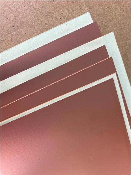
TP2500 2-layer 0.8mm PCB is a rigid high frequency printed circuit board fabricated on fiberglass-free PPO ceramic thermoplastic TP2500 copper clad laminate. TP series substrate is a special thermoplastic high-frequency material composed of ceramic filler and polyphenylene oxide (PPO) resin without fiberglass reinforcement. The dielectric constant of TP laminate can be precisely customized by adjusting the mixing ratio of ceramic powder and PPO resin. This 0.9mm finished thickness TP2500 PCB delivers low dielectric loss and reliable electrical performance for compact RF circuits, and serves as a cost-effective alternative to ceramic substrates for miniaturized antenna designs.
.jpg)
2. Features
- Customizable dielectric constant Dk from 3 to 25 with stable dielectric performance; common grades include TP300, TP440, TP600, TP615, TP920, TP960, TP2500
- Low dielectric loss; loss rises slightly with frequency and remains stable below 10GHz
- Long-term operating temperature: -100°C ~ +150°C, excellent low-temperature resistance; material deformation and copper peel risk above 180°C
- Minimum available thickness of 0.5mm, multiple thickness options for custom PCB fabrication
- Radiation resistant and low outgassing properties
- Superior copper-dielectric adhesion compared with vacuum coated ceramic substrates
- Easy machining, supports drilling, turning, grinding, shearing and etching
3. Benefits
- Fiberglass-free structure eliminates weave effect for consistent RF signal transmission on 2-layer TP2500 RF PCB
- Wide customizable dielectric constant range from Dk 3 to 25 for miniaturized circuit design of 0.9mm TP2500 high frequency PCB
- Excellent machinability, supports multiple machining operations, easier processing than pure ceramic substrates for TP2500 microwave PCB
- Reliable copper foil adhesion compared with vacuum-coated ceramic substrates for this 0.8mm core TP2500 rigid PCB
- Radiation resistance and low outgassing performance for harsh working environments of TP2500 thermoplastic PCB
- Lower manufacturing cost than ceramic dielectric substrates for antenna and navigation applications of TP2500 PCB
- 4. PCB Construction details
| Item | Specification |
| Base material | TP2500 |
| Layer count | 2-layer rigid |
| Board dimensions | 78 mm x 43.05 mm=1PCS, +/- 0.15mm |
| Minimum Trace/Space | 6/8 mils |
| Minimum Hole Size | 0.25mm |
| Blind vias | No |
| Finished board thickness | 0.9mm |
| Finished Cu weight | 1oz (1.4 mils) outer layers |
| Via plating thickness | 20 μm |
| Surface finish | Pure gold plating (Nickel free) |
| Top Silkscreen | NO |
| Bottom Silkscreen | No |
| Top Solder Mask | NO |
| Bottom Solder Mask | No |
| Pre-shipment test | 100% Electrical test used prior to shipment |
5. PCB Stackup: 2-layer rigid PCB
- Copper_layer_1 - 35 μm
- TP2500 Core - 0.8 mm
- Copper_layer_2 - 35 μm
6. PCB Statistics
- Components: 26
- Total Pads: 49
- Thru Hole Pads: 27
- Top SMT Pads: 22
- Bottom SMT Pads: 0
- Vias: 36
- Nets: 1
7. Type of artwork supplied
Gerber RS-274-X
8. Quality standard
IPC-Class-2
9. Availability
Worldwide
10. Some Typical Applications
- Beidou navigation systems
- Missile-borne equipment
- Fuzes
- Miniaturized antennas
11. TP & TP2500 Microwave Composite Dielectric Copper Clad Laminate Knowledge
TP series is a unique fiberglass-free thermoplastic high-frequency CCL. Its dielectric layer is formulated with ceramic powder and PPO resin, and the dielectric constant can be precisely tuned by adjusting ceramic and PPO proportions. TP stands for unclad base material; TP-1 is single-sided copper clad laminate, TP-2 is double-sided copper clad laminate. The 2-layer TP2500 PCB adopts TP-2 type copper clad laminate as its core dielectric material.
11.1 Core Electrical & Material Features
- Customizable Dk range from 3 to 25 with stable dielectric performance; common grades include TP300, TP440, TP600, TP615, TP920, TP960, TP2500. 0.8mm TP2500 substrate is ideal for compact RF PCB fabrication
- Low dielectric loss; loss rises slightly with frequency and remains stable below 10GHz, ideal for 0.9mm TP2500 RF circuit board
- Long-term operating temperature range: -100°C ~ +150°C; material deformation and copper peel risk above 180°C for TP2500 high frequency PCB
- Radiation resistant and low outgassing properties, suitable for high-reliability TP2500 microwave PCB
- Ultra-low moisture absorption, stable electrical parameters under variable humidity for TP2500 thermoplastic PCB
11.2 Processing & Structural Advantages
- Excellent machinability, supports drilling, turning, grinding, shearing and etching, much easier to process than ceramic substrates for 2-layer TP2500 PCB
- Superior copper-dielectric adhesion compared with vacuum coated ceramic substrates for this 0.9mm TP2500 rigid PCB
- Minimum available thickness of 0.5mm, multiple thickness options for custom TP2500 high frequency PCB requirements
- Thermoplastic processing, high fabrication yield and lower cost than ceramic substrates for 0.8mm core TP2500 RF PCB
- Multilayer stacking is not generally recommended; if required, low-temperature bonding sheets must be used and feasibility fully verified for custom TP2500 PCB
11.3 Soldering Limitations & Application Notes
- Not suitable for 260°C thermal shock test or wave soldering when manufacturing TP2500 microwave PCB
- Hand soldering with constant-temperature iron is recommended for assembling 2-layer TP2500 thermoplastic PCB
- Reflow soldering is not advised; if necessary, peak temperature should stay below 200°C with full pre-production evaluation of the TP2500 PCB
12. TP2500 DataSheet
| Product Model/Data | Property | Test Condition | Unit | TP2500 |
| TP2500 | Dielectric Constant | 5GHz | / | 25.0±1.0 |
| Dielectric Constant Tolerance | / | / | ±4% | |
| Dissipation Factor | 5GHz | / | 0.0020~0.0025 | |
| Temperature Coefficient of Dielectric Constant | -55 ~150℃ | PPM/℃ | -55 | |
| Peel Strength | 1 OZ Normal Condition | N/mm | >0.6 | |
| Peel Strength | 1 OZ After Alternating Humid Heat | N/mm | >0.4 | |
| Volume Resistivity | Normal Condition, 500V | MΩ.cm | >1×10⁹ | |
| Surface Resistivity | Normal Condition, 500V | MΩ | >1×10⁷ | |
| Coefficient of Thermal Expansion (X Y Z) | -55 ~150℃ | PPM/℃ | 35,35,40 | |
| Water Absorption | 20±2℃, 24 hours | % | ≤0.01 | |
| Continuous Operating Temperature | Temperature Chamber | ℃ | -100~150℃ | |
| Material Composition | / | / | Polyphenylene oxide, ceramic, with ED copper foil | |
| Density | / | g/cm3 | 2.94 | |
| Thermal Conductivity | / | W/(M.K) | 1.0 |
13. Product Summary
TP2500 2-Layer high frequency PCB is a rigid printed circuit board built on 0.8mm TP2500 fiberglass-free PPO ceramic thermoplastic copper clad laminate. Wangling 0.9mm finished thickness TP2500 PCB uses nickel-free pure gold plating surface finish, no solder mask and no silkscreen on both sides. 0.8 mm TP2500 core PCB undergoes 100% electrical testing before shipment. Thanks to fiberglass-free PPO ceramic composite structure, TP2500 RF PCB is widely used for Beidou navigation systems, missile-borne equipment, fuze devices and miniaturized antenna applications.
14. Application
The 2-layer 0.9mm TP2500 high frequency PCB is widely deployed in Beidou navigation, missile-borne electronics, fuze systems and compact miniaturized antenna modules. This TP2500 thermoplastic PCB features fiberglass-free PPO ceramic composite structure, making the 0.8mm core TP2500 microwave PCB ideal for RF systems that demand stable dielectric performance, small form factor and low outgassing capability.