


 Home
-
F4B PCB
-
Double-Layer F4BTMS450 HASL Lead-Free Rigid PCB 20mil Ceramic-Filled PTFE Laminate for Aerospace & Radar Applications
Home
-
F4B PCB
-
Double-Layer F4BTMS450 HASL Lead-Free Rigid PCB 20mil Ceramic-Filled PTFE Laminate for Aerospace & Radar Applications
Double-Layer F4BTMS450 HASL Lead-Free Rigid PCB 20mil Ceramic-Filled PTFE Laminate for Aerospace & Radar Applications
Printed Circuit Boards are custom-made products; the images and specifications provided are for reference only.
1. Product Introduction
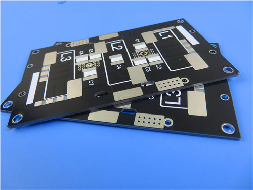
F4BTMS450 2-layer rigid high frequency PCB is an upgraded aerospace-grade circuit board built on advanced F4BTMS series ceramic-filled PTFE substrate technology. Featuring a 0.6mm finished board thickness and reliable Lead-Free Hot Air Solder Leveling (HASL LF) surface finish, this precision high frequency PCB adopts ultra-thin and ultra-fine fiberglass cloth reinforcement combined with uniformly dispersed nano-ceramic fillers, effectively eliminating the negative impact of fiberglass on electromagnetic wave transmission. Manufactured with standard Gerber RS-274-X artwork and compliant with strict IPC-Class-2 quality criteria, every F4BTMS450 PCB undergoes 100% electrical testing before shipment to guarantee consistent performance stability. With ultra-low dielectric loss, minimized thermal anisotropy, and excellent high-frequency stability up to 40GHz, this 2-layer rigid PCB offers worldwide availability and serves as a perfect domestic alternative to imported high-frequency substrates for military radar, satellite communication, and aerospace electronic systems.
2. Core Product Features
Engineered for extreme high-frequency, high-temperature, and aerospace working environments, the F4BTMS450 high frequency PCB integrates upgraded material formulation and optimized manufacturing processes, delivering comprehensive superior technical features for precision RF circuit design:
- Precise and stable dielectric constant (Dk) of 4.5 ±0.09 at 10GHz, achieving outstanding batch consistency and tight parameter tolerance
- Ultra-low dissipation factor of 0.0015 at 10GHz and 0.0019 at 20GHz, maintaining low-loss signal transmission across broadband high-frequency bands
- Superior low thermal expansion performance with X-axis and Y-axis CTE of 12 ppm/°C and Z-axis CTE of 45 ppm/°C within -55°C to 288°C, ensuring excellent dimensional stability
- Low DK thermal coefficient of -58 ppm/°C ranging from -55°C to 150°C, stabilizing dielectric performance under variable temperature conditions
- Reliable UL-94 V0 flame retardant rating, meeting industrial and aerospace safety standards
- Enhanced thermal conductivity of 0.64 W/MK, effectively improving heat dissipation for high-power circuit applications
- Ultra-low moisture absorption rate of 0.08%, preventing performance degradation caused by humid environmental conditions
- Standard RTF low-roughness copper foil configuration that reduces conductor loss and maintains durable copper peel strength
- Excellent radiation resistance and low outgassing properties, fully compliant with aerospace vacuum environment application requirements
- Minimized X/Y/Z directional anisotropy, eliminating signal deviation caused by structural performance differences
3. Product Performance Benefits
Benefiting from the innovative ceramic-filled PTFE formula and ultra-fine fiberglass reinforcement structure, the F4BTMS450 2-layer high frequency PCB provides remarkable practical advantages for high-end high-frequency electronic manufacturing:
- Greatly suppresses the fiberglass effect during electromagnetic wave propagation, realizing ultra-low dielectric loss and higher signal transmission efficiency at high frequencies
- Delivers consistent dielectric constant and loss stability up to 40GHz, perfectly adapting to phase-sensitive antenna and high-precision RF circuit applications
- Balanced low CTE in all directions effectively avoids board deformation and plated-through-hole failure under extreme temperature changes
- Stable dielectric temperature characteristics ensure consistent frequency and phase performance in fluctuating thermal environments
- Superior radiation resistance and low outgassing capability make it reliable for long-term service in aerospace vacuum and radiation environments
- Compatible with copper and aluminum base substrates, supporting diversified high-power circuit structural designs
- Excellent machinability for fine-line, dense-hole, and multi-layer PCB processing, meeting high-precision customization demands
- High overall material consistency and repeatability, lowering production failure rates and improving product yield
4. PCB Construction Details
F4BTMS450 high frequency rigid PCB is produced with standardized high-precision manufacturing parameters. All construction specifications are organized in the table below for design, production and inspection reference:
| Technical Item | Detailed Specification |
| Base Material | F4BTMS450 Upgraded Ceramic-Filled PTFE Substrate |
| Layer Count | 2-Layer Rigid PCB |
| Board Dimensions | 38.4mm x 56.35mm (1PCS), Dimension Tolerance: +/- 0.15mm |
| Minimum Trace / Space | 4/6 mils |
| Minimum Hole Size | 0.3mm |
| Blind Vias Design | No Blind Vias Applied |
| Finished Board Thickness | 0.6mm |
| Finished Copper Weight | 1oz (1.4 mils) |
| Via Plating Thickness | 20 μm |
| Surface Finish | HASL LF (Lead-Free Hot Air Solder Leveling) |
| Top Silkscreen | White |
| Bottom Silkscreen | No Silkscreen |
| Top Solder Mask | Black Solder Mask |
| Bottom Solder Mask | No Solder Mask |
| Pre-Shipment Inspection | 100% Full Electrical Testing |
5. PCB Stackup Structure
This 2-layer rigid high frequency PCB adopts a scientific and stable layer stackup structure with premium F4BTMS450 core substrate and low-loss copper layers, ensuring balanced electrical and mechanical performance:
- Copper_layer_1: 35 μm Low Roughness RTF Copper Foil
- F4BTMS450 Core Substrate: 0.508 mm (20mil)
- Copper_layer_2: 35 μm Low Roughness RTF Copper Foil
6. PCB Circuit Statistics
The F4BTMS450 high frequency PCB features a compact and precise circuit layout with complete component and wiring configurations, meeting high-precision assembly and high-frequency circuit design standards:
- Total Mountable Components: 13
- Total Circuit Pads: 20
- Through Hole Pads: 12
- Top SMT Pads: 8
- Bottom SMT Pads: 0
- Conductive Vias: 9
- Circuit Nets: 5
7. Production Specification & Global Supply
All F4BTMS450 2-layer high frequency PCBs are produced based on standard Gerber RS-274-X artwork format, achieving universal compatibility with global PCB processing, testing and assembly equipment. The entire manufacturing process strictly complies with IPC-Class-2 industrial quality standards to guarantee high dimensional accuracy, stable electrical performance and long-term structural reliability. With stable worldwide supply capacity, this aerospace-grade high frequency PCB can provide standardized and customized circuit board solutions for aerospace, military defense, satellite communication and high-end RF microwave enterprises globally.
8. Typical Application Scenarios
Supported by ultra-low dielectric loss, excellent thermal stability, radiation resistance and vacuum low-outgassing performance, F4BTMS450 high frequency PCB is widely adopted in high-end aerospace and military high-frequency electronic fields:
- Aerospace Equipment: Space devices, cabin electronic systems and aviation onboard equipment
- High-Frequency Electronic Systems: Microwave circuits and full-band RF application modules
- Defense Equipment: Military radar systems and precision signal processing devices
- Antenna Systems: Feed networks, phase-sensitive antennas and phased array antenna arrays
- Communication Devices: High-precision satellite communication terminal equipment
9. F4BTMS450 Substrate Professional Knowledge
F4BTMS450 is a high-end upgraded ceramic-filled PTFE ultra-fine fiberglass composite substrate, iteratively optimized on the basis of the traditional F4BTM series. It achieves comprehensive upgrades in material formulation and manufacturing processes, solving multiple performance drawbacks of conventional PTFE substrates. Below is a detailed breakdown of its substrate composition, structural advantages, processing features and environmental reliability:
9.1 Material Upgrade & Grade Positioning
As a new-generation upgraded member of the F4BTMS material family, F4BTMS450 breaks through the technical limitations of classic F4BTM series substrates. It adopts a customized formula with high-content uniformly distributed nano-ceramic fillers and ultra-thin ultra-fine fiberglass cloth reinforcement. This innovative structural optimization greatly improves overall material stability, dielectric uniformity and mechanical reliability. With aerospace-grade high-reliability performance, F4BTMS450 can completely replace imported high-frequency substrates and is widely recognized as a premium domestic alternative for military and aerospace high-precision circuit applications.
9.2 Unique Structural Design & Electromagnetic Advantages
Different from ordinary thick fiberglass reinforced PTFE laminates, F4BTMS450 adopts a low-dose ultra-fine fiberglass matching scheme, combined with high-proportion dispersed nano-ceramic particles blended with PTFE resin. This scientific composite structure greatly weakens the fiberglass interference effect on electromagnetic wave propagation, fundamentally reducing high-frequency dielectric loss and signal attenuation. In addition, the optimized formula significantly lowers X/Y/Z three-dimensional thermal anisotropy, effectively broadening the effective working frequency band up to 40GHz. It also enhances the substrate’s electrical strength and thermal conductivity, while maintaining ultra-low thermal expansion coefficient and stable dielectric temperature characteristics across wide temperature ranges from -55°C to 150°C.
9.3 Standard Configuration & Structural Compatibility
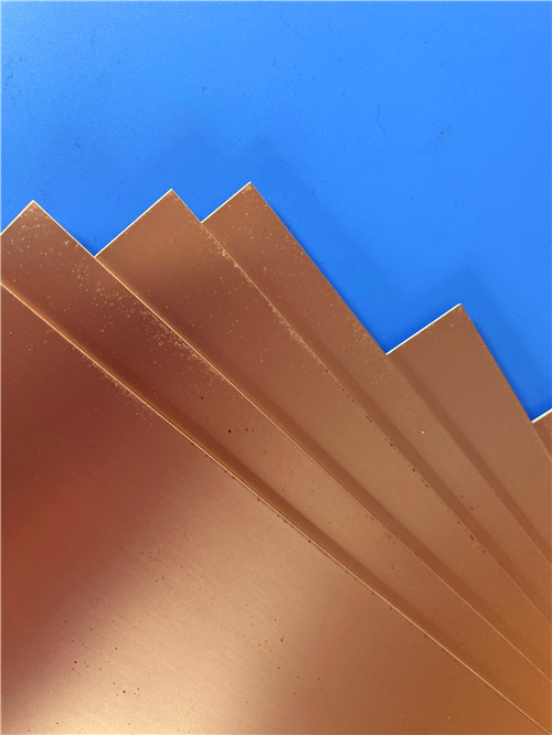
F4BTMS450 substrate is factory-standardized with high-quality RTF low-roughness copper foil. The low-profile copper foil design greatly reduces high-frequency conductor loss, while maintaining excellent and durable copper peel strength to ensure long-term circuit bonding reliability. The substrate features strong structural compatibility and can be flexibly matched with copper base or aluminum base materials, perfectly adapting to high-power heat-dissipation microwave and RF circuit designs. It supports composite structural customization for diverse high-power electronic equipment.
9.4 Processing Performance & Customization Feasibility
This ceramic-filled PTFE substrate is fully compatible with standard industrial PTFE PCB processing technologies. It delivers outstanding manufacturability for fine-line etching, dense hole drilling, multi-layer lamination and backplane processing. The stable physical properties enable high-precision and high-complexity PCB customization, effectively improving production yield and supporting mass manufacturing of high-density high-frequency circuit boards for aerospace and military projects.
9.5 Extreme Environmental Reliability Performance
F4BTMS450 laminate features ultra-tight dielectric constant tolerance and excellent batch-to-batch consistency, ensuring stable and unified circuit performance in mass production. It possesses ultra-low outgassing properties that fully meet aerospace vacuum application standards. Meanwhile, the material delivers superior radiation resistance, maintaining stable physical structure and dielectric parameters even after long-term exposure to ionizing radiation and extreme temperature environments. These comprehensive reliable properties make F4BTMS450 the ideal substrate for phase-sensitive, high-precision and high-reliability aerospace, defense and satellite communication high-frequency circuit systems.
Different from conventional fiberglass-reinforced PTFE laminates, F4BTMS450 adopts a low-dose ultra-fine fiberglass matching with high uniformly dispersed nano-ceramic particles mixed in PTFE resin. This design greatly weakens the fiberglass interference effect on electromagnetic wave propagation, significantly reducing high-frequency dielectric loss. Meanwhile, it effectively reduces X/Y/Z three-dimensional thermal anisotropy, expands the effective working frequency band, improves material electrical strength and thermal conductivity, and maintains ultra-low thermal expansion coefficient and excellent dielectric temperature stability in wide temperature ranges.
F4BTMS450 substrate is standardized with premium RTF low-roughness copper foil, which effectively reduces high-frequency conductor loss while retaining outstanding copper foil peel strength. The versatile substrate can be matched with copper base or aluminum base materials to adapt to high-power heat-dissipation circuit designs. In addition, the material supports standard PTFE PCB processing technology, with excellent processability for fine lines, dense holes, multi-layer stacking and backplane processing, delivering high feasibility for high-precision and high-complexity PCB customization.
With ultra-tight dielectric tolerance, excellent batch consistency, ultra-low outgassing and superior radiation resistance, F4BTMS450 maintains stable physical and dielectric properties under extreme temperature, vacuum and radiation environments. These irreplaceable advantages make it the preferred substrate for phase-sensitive, high-precision and high-reliability aerospace and military high-frequency circuit systems.
10. Product Summary
F4BTMS450 2-Layer high frequency PCB is an upgraded aerospace-grade rigid microwave circuit board built on ceramic-filled ultra-fine fiberglass PTFE substrate. Featuring 0.6mm finished thickness, reliable HASL LF surface treatment, stable Dk 4.5 dielectric performance and ultra-low high-frequency loss, this 2-layer rigid PCB delivers low thermal expansion, minimal anisotropy, excellent radiation resistance and vacuum low-outgassing performance. Complying with IPC-Class-2 standards and 100% pre-delivery electrical testing, it supports high-precision fine-line processing and high-power circuit design. As a cost-effective imported substitute substrate with global supply capability, it is ideal for military radar, phased array antennas, satellite communications and aerospace high-frequency electronic equipment manufacturing.
11. F4BTMS450 Datasheet
| Product Characteristics | Test Condition | Unit | F4BTMS450 |
| Dielectric Constant (Typical Value) | 10 GHz | — | 4.50 |
| Dielectric Constant Tolerance | — | — | ±0.09 |
| Dielectric Constant (Design Value) | 10 GHz | — | 4.5 |
| Dissipation Factor (Typical Value) | 2 GHz | — | 0.0015 |
| Dissipation Factor (Typical Value) | 10 GHz | — | 0.0019 |
| Dissipation Factor (Typical Value) | 20 GHz | — | 0.0024 |
| Temperature Coefficient of Dielectric Constant | -55℃ ~ 150℃ | PPM/℃ | -58 |
| Peel Strength | 1 OZ RTF Copper Foil | N/mm | >1.2 |
| Volume Resistivity | Ambient Condition | MΩ·cm | ≥1×10⁸ |
| Surface Resistance | Ambient Condition | MΩ | ≥1×10⁸ |
| Dielectric Strength (Z-axis) | 5KW, 500V/s | KV/mm | >45 |
| Breakdown Voltage (XY-plane) | 5KW, 500V/s | KV | >54 |
| Coefficient of Thermal Expansion (X, Y-axis) | -55℃ ~ 288℃ | ppm/℃ | 12, 12 |
| Coefficient of Thermal Expansion (Z-axis) | -55℃ ~ 288℃ | ppm/℃ | 45 |
| Thermal Stress | 260℃, 10s, 3 cycles | — | No Delamination |
| Water Absorption | 20±2℃, 24 hours | % | 0.08 |
| Density | Ambient Temperature | g/cm³ | 2.53 |
| Long-term Operating Temperature | Temperature Chamber | ℃ | -55 ~ +260 |
| Thermal Conductivity | Z-axis | W/(m·K) | 0.64 |
| Flame Retardancy | — | UL-94 | V-0 |
| Material Composition | — | — | PTFE, ultra-thin ultra-fine fiberglass cloth, ceramic |