


 Home
-
F4B PCB
-
F4BME275 2-Layer 1.6mm Pure Gold PCB High Frequency RF Laminate PCB for Radar & Satellite Communication
Home
-
F4B PCB
-
F4BME275 2-Layer 1.6mm Pure Gold PCB High Frequency RF Laminate PCB for Radar & Satellite Communication
F4BME275 2-Layer 1.6mm Pure Gold PCB High Frequency RF Laminate PCB for Radar & Satellite Communication
Printed Circuit Boards are custom-made products; the images and specifications provided are for reference only.
1. Product Introduction
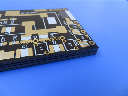
F4BME275 2-layer high-frequency RF PCB is a next-generation high-performance rigid circuit board optimized for professional microwave and radio frequency electronic systems. Built on upgraded F4BME275 PTFE fiberglass composite laminate, this 1.6mm thick RF PCB adopts premium 5um (197u”) pure gold surface finishing to deliver superior conductivity, oxidation resistance and assembly reliability. Fabricated with industry-standard Gerber RS-274-X artwork and manufactured in compliance with IPC-Class-2 quality standards, every finished board undergoes 100% full electrical testing before shipment to ensure stable and consistent circuit performance. Equipped with high-quality Reverse-Treated Foil (RTF) copper, this custom RF PCB features low conductor loss and outstanding low-PIM characteristics, serving as a high-cost-performance domestic alternative to imported high-frequency substrates. With worldwide supply availability, it is widely applicable for radar systems, phased array antennas, base station equipment and satellite communication devices.
2. Core Product Features
Tailored for high-precision RF and microwave working scenarios, F4BME275 high frequency PCB integrates upgraded PTFE fiberglass composite formula and standardized manufacturing processes, delivering balanced electrical and mechanical advantages:
- Customizable dielectric constant range from 2.17 to 3.0 via adjustable PTFE and fiberglass ratio, supporting diversified high-frequency circuit design demands
- Ultra-low dielectric loss and enhanced insulation resistance, achieving more stable high-frequency signal transmission than traditional F4B series substrates
- Premium RTF reverse-treated copper foil configuration provides excellent low-PIM performance, ideal for high-sensitivity RF signal circuits
- Supports ultra-fine precise etching processing, enabling high-precision fine-line circuit layout and improving circuit integration
- Optimized fiberglass content enhances dimensional stability and reduces thermal expansion coefficient, effectively lowering temperature drift impact
- Excellent radiation resistance and low outgassing properties, adapting to long-term stable operation in complex electromagnetic environments
- Diversified panel size options, maximizing material utilization and reducing overall production costs
- Mature commercial mass production process with stable batch consistency and outstanding cost-performance ratio
3. Product Performance Benefits
Benefiting from the scientific PTFE fiberglass composite structure and RTF copper foil design, the F4BME275 2-layer RF PCB provides comprehensive practical advantages for modern high-frequency electronic product development:
- Precisely adjustable DK value realizes flexible performance matching, allowing engineers to balance electrical performance, mechanical stability and processing requirements freely
- Low conductor loss and low dielectric loss design greatly reduce high-frequency signal attenuation, improving transmission efficiency of microwave and RF circuits
- Superior low-PIM performance effectively avoids signal interference and distortion, ensuring high precision of phase-sensitive circuit equipment
- Enhanced dimensional stability and low thermal expansion coefficient minimize board deformation and parameter drift under variable temperature conditions
- Upgraded performance comprehensively surpasses traditional F4B220 substrates, fully replacing imported high-frequency laminates to reduce procurement costs
- High processing compatibility supports fine-line precision processing and standardized mass production, improving product yield for high-frequency module manufacturing
- Excellent environmental adaptability with radiation resistance and low outgassing, suitable for outdoor base stations, aerospace and communication equipment working in harsh environments
4. PCB Construction Details
This custom F4BME275 high-frequency RF PCB adopts standardized high-precision production parameters. All core construction specifications are sorted in the table below for design, production and inspection reference:
| Technical Item | Detailed Specification |
| PCB Type | 2-Layer Rigid RF High Frequency PCB |
| Board Dimensions | 103mm x 76mm (1PCS), Dimension Tolerance: +/- 0.15mm |
| Minimum Trace / Space | 6/9 mils |
| Minimum Hole Size | 0.5mm |
| Finished Board Thickness | 1.6mm |
| Finished Outer Layer Copper Weight | 1oz (1.4 mils) |
| Via Plating Thickness | 20 μm |
| Surface Finish | Pure Gold 5μm (197u") |
| Top Silkscreen | White |
| Bottom Silkscreen | No Silkscreen Printing |
| Top Solder Mask | Black Solder Mask |
| Bottom Solder Mask | No Solder Mask Coating |
| Pre-Shipment Quality Test | 100% Full Electrical Performance Testing |
5. PCB Stackup Structure
This 2-layer rigid high frequency RF PCB adopts a stable and scientific layer stackup structure with authentic F4BME275 core substrate and high-performance RTF copper layers, ensuring uniform electrical transmission and structural stability:
- Copper_layer_1: 35 μm Reverse-Treated Foil (RTF) Copper
- F4BME275 Core Substrate: 1.524 mm (60mil)
- Copper_layer_2: 35 μm Reverse-Treated Foil (RTF) Copper
6. PCB Circuit Statistics
The F4BME275 high frequency RF PCB features a refined and compact circuit layout with complete component assembly and wiring configurations, meeting high-precision RF circuit design and assembly standards:
- Total Mountable Components: 37
- Total Circuit Pads: 56
- Through Hole Pads: 37
- Top SMT Pads: 19
- Bottom SMT Pads: 0
- Conductive Vias: 21
- Circuit Nets: 7
7. Production Specification & Global Supply
All F4BME275 2-layer high frequency RF PCBs are produced with standard Gerber RS-274-X artwork format, achieving full compatibility with global mainstream PCB processing, testing and assembly equipment. The entire manufacturing process strictly implements IPC-Class-2 industrial quality standards to ensure high dimensional accuracy, stable dielectric performance and long-term structural reliability. With mature and stable worldwide supply channels, this high-performance PTFE laminate PCB can provide standardized and customized circuit board solutions for RF microwave enterprises, communication equipment manufacturers and defense electronic factories across the globe.
8. Typical Application Scenarios
Supported by low dielectric loss, excellent low-PIM performance, stable high-frequency transmission and superior environmental adaptability, F4BME275 RF PCB is widely used in high-end communication and microwave electronic fields:
- High-Frequency Electronic Systems: Microwave circuits, full-band RF modules and radar system equipment
- Passive RF Components: Phase shifters, power dividers, signal couplers and combiners
- Antenna Systems: Feed networks, phased array antennas and base station antenna equipment
- Communication Equipment: Satellite communication terminals and outdoor wireless communication devices
9. F4BME275 Substrate Professional Knowledge
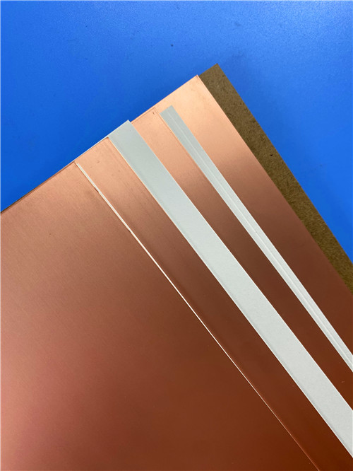
F4BME275 is an upgraded high-performance PTFE fiberglass cloth copper-clad laminate, optimized and iterated on the basis of traditional F4B and F4B220 series materials. It adopts a scientific composite formula composed of high-quality fiberglass cloth, PTFE resin and PTFE film, combined with rigorous high-pressure molding processes to achieve comprehensive performance upgrades. Compared with traditional substrates, F4BME275 features wider adjustable dielectric constant range, lower high-frequency loss, higher insulation resistance and more stable operational performance, which can fully replace imported equivalent high-frequency laminates for commercial and industrial high-precision RF applications.
9.1 F4BM & F4BME Series Difference
F4BM and F4BME series substrates share the same dielectric core layer material, while the core difference lies in the matching copper foil type. The F4BM substrate is equipped with conventional ED copper foil, suitable for ordinary RF circuit scenarios without strict PIM performance requirements. In contrast, the upgraded F4BME275 substrate adopts premium reverse-treated RTF copper foil, which delivers excellent low-PIM characteristics, more accurate circuit etching precision and lower high-frequency conductor loss, fully meeting the stringent requirements of high-sensitivity communication circuits.
9.2 Material Formula & Tuning Principle
F4BME275 realizes precise dielectric constant tuning by scientifically adjusting the mixing ratio of PTFE resin and fiberglass cloth. Increasing fiberglass content will appropriately raise the dielectric constant, significantly enhance substrate dimensional stability, reduce thermal expansion coefficient and suppress temperature drift of electrical parameters. Meanwhile, the higher fiberglass ratio brings only marginal increase in dielectric loss, achieving an optimal balance between low-loss performance and mechanical stability. This flexible tuning feature allows design engineers to select the most suitable material grade according to actual circuit demands.
9.3 Core Structural & Process Advantages
The RTF reverse-treated copper foil equipped on F4BME275 effectively reduces high-frequency conductor loss and improves signal transmission efficiency. The material supports ultra-fine line precision etching, realizing high-density and high-precision circuit layout. In addition, diversified standard panel size options greatly improve material utilization rate, effectively reducing customized PCB production costs while ensuring processing feasibility of fine lines and dense holes.
9.4 Environmental & Industrial Reliability
F4BME275 substrate possesses excellent radiation resistance and ultra-low outgassing properties, maintaining stable physical structure and dielectric parameters in complex electromagnetic and vacuum environments. With mature commercial mass production technology, it features excellent batch consistency and cost-performance ratio, supporting large-scale standardized production of high-frequency communication equipment and industrial microwave devices.
10. Product Summary
F4BME275 2-Layer high frequency RF PCB is an upgraded commercial-grade PTFE fiberglass composite rigid circuit board for microwave and RF applications. Featuring 1.6mm finished thickness, premium 5μm pure gold surface treatment, customized DK 2.17-3.0 adjustable dielectric constant and low-loss RTF copper structure, this 2-layer PCB delivers excellent low-PIM performance, high dimensional stability and outstanding temperature drift resistance. Upgraded from traditional F4B220 substrates and compliant with IPC-Class-2 quality standards, it supports high-precision fine-line processing and mass production. With global availability and superior cost performance, it is the ideal alternative to imported substrates for radar systems, phased array antennas, power divider components and satellite communication equipment.
11. Datasheet
| Product Characteristics | Test Condition | Unit | F4BM275 | F4BME275 |
| Dielectric Constant (Typical Value) | 10 GHz | — | 2.75 | 2.75 |
| Dielectric Constant Tolerance | — | — | ±0.05 | ±0.05 |
| Dissipation Factor (Typical Value) | 10 GHz | — | 0.0015 | 0.0015 |
| Dissipation Factor (Typical Value) | 20 GHz | — | 0.0021 | 0.0021 |
| Temperature Coefficient of Dielectric Constant | -55℃ ~ 150℃ | PPM/℃ | -92 | -92 |
| Peel Strength | 1 OZ ED Copper Foil | N/mm | >1.8 | — |
| Peel Strength | 1 OZ Reverse RTF Copper Foil | N/mm | — | >1.6 |
| Volume Resistivity | Ambient Condition | MΩ·cm | ≥6×10⁶ | ≥6×10⁶ |
| Surface Resistance | Ambient Condition | MΩ | ≥1×10⁶ | ≥1×10⁶ |
| Dielectric Strength (Z-axis) | 5KW, 500V/s | KV/mm | >28 | >28 |
| Breakdown Voltage (XY-plane) | 5KW, 500V/s | KV | >35 | >35 |
| Coefficient of Thermal Expansion (XY-axis) | -55℃ ~ 288℃ | ppm/℃ | 14, 16 | 14, 16 |
| Coefficient of Thermal Expansion (Z-axis) | -55℃ ~ 288℃ | ppm/℃ | 112 | 112 |
| Thermal Stress | 260℃, 10s, 3 cycles | — | No Delamination | No Delamination |
| Water Absorption | 20±2℃, 24 hours | % | ≤0.08 | ≤0.08 |
| Density | Ambient Temperature | g/cm³ | 2.28 | 2.28 |
| Long-term Operating Temperature | Temperature Chamber | ℃ | -55 ~ +260 | -55 ~ +260 |
| Thermal Conductivity | Z-axis | W/(m·K) | 0.38 | 0.38 |
| PIM Value | RTF Copper Foil Only | dBc | — | ≤-159 |
| Flame Retardancy | — | UL-94 | V-0 | V-0 |
| Material Composition | — | — | PTFE + Fiberglass Cloth(Matched with ED Copper Foil) | PTFE + Fiberglass Cloth(Matched with Reverse RTF Copper Foil) |