


 Home
-
F4B PCB
-
F4BM233 2-Layer Immersion Gold PCB 4mm F4BM233 Laminate with 1oz Copper for RF and Microwave Application
F4BM233 2-Layer Immersion Gold PCB 4mm F4BM233 Laminate with 1oz Copper for RF and Microwave Application
Printed Circuit Boards are custom-made products; the images and specifications provided are for reference only.
1. Product Overview of F4BM233 2-Layer PCB
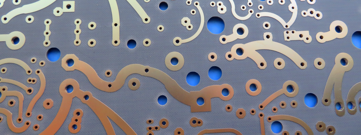
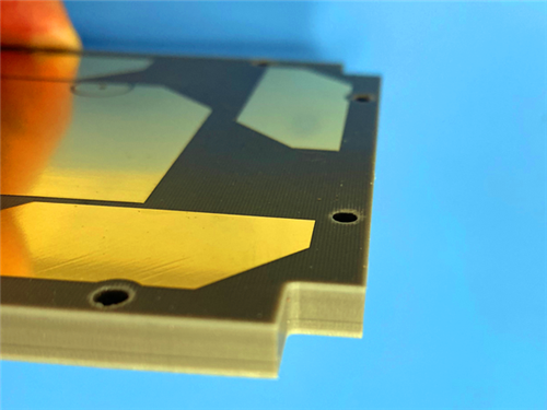
F4BM233 2-Layer PCB is a custom rigid high frequency PCB fabricated from 4mm F4BM233 copper clad laminate. F4BM233 PCB comes with 4mm substrate and 1oz finished copper thickness, and it adopts differentiated solder mask construction. The top layer features green solder mask without silk screen characters, while the bottom layer is manufactured with no solder mask and no silk screen characters. Immersion gold is selected as the surface finish, which improves solderability, oxidation resistance and electrical conductivity for stable long-term operation. The finished dimension of this PCB is 65mm x 72mm per piece with tight dimensional tolerance and stable mechanical performance.
As a professional high frequency circuit board, F4BM233 2-Layer PCB is designed for high-speed signal transmission, microwave and RFapplications. It retains the low dielectric loss and high stability properties of F4BM233 substrate to reduce signal attenuation and frequency drift under high frequency conditions. The symmetrical stackup design balances mechanical and electrical performance, making it a cost-effective alternative to imported high frequency PCB for commercial and industrial wireless communication projects.
2. F4BM233 PCB Core Specification Parameters
The detailed technical parameters of the 2-layer 4mm F4BM233 high frequency PCB are sorted in the table below for clear reference:
| Parameter Item | Specification Details |
| Base Material | |
| F4BM233 High Frequency Copper Clad Laminate | |
| Layer Count | 2-Layer Rigid PCB |
| Substrate Thickness | 4mm |
| Finished Copper Thickness | 1Oz |
| Top Layer Treatment | |
| Green Solder Mask, No Silk Screen | |
| Bottom Layer Treatment | No Solder Mask, No Silk Screen |
| Surface Finishing | Immersion Gold |
| Product Dimension | 65mm × 72mm |
| Unit Quantity | 1PCS |
3. PCB Stackup Structure
F4BM233 2-layer rigid PCB adopts standard symmetrical stackup design to guarantee consistent electrical performance and mechanical stability:
- Copper_layer_1 – 1oz (35 μm)
- F4BM233 Core – 4mm
- Copper_layer_2 – 1oz (35 μm)
4.F4BM Series and F4BME Series Copper Clad Laminate Material Knowledge
4.1 Material Overview
F4BM series (including F4BM233) and F4BME series are PTFE fiberglass cloth copper-clad laminates for high frequency and microwave PCB fabrication. Both are manufactured with PTFE resin, fiberglass cloth and PTFE film through strict lamination processes, delivering better electrical performance than conventional F4B substrates, including wider tunable dielectric constant range, low dielectric loss, high insulation resistance and stable high-frequency characteristics. Though they share the same dielectric base formulation, F4BM series and F4BME series are separate product lines defined by different copper foil selections and target performance requirements.
F4BM series uses ED electrodeposited copper foil, suited for general RFand microwave projects without strict PIM requirements. F4BM233 is a specific grade inside the F4BM series, tuned to a fixed dielectric constant for designated high-frequency designs. F4BME series adopts reverse-treated RTF copper foil to achieve superior PIM performance, tighter impedance control and lower conductor loss, which serves high-precision passive RFcircuits and base station applications.
Dielectric constant of each laminate grade is controlled by adjusting the ratio of PTFE resin and fiberglass cloth. This formulation balances low signal attenuation and good dimensional stability. Within the adjustable DK range, higher fiberglass loading produces higher dielectric constant, better dimensional stability, lower thermal expansion coefficient and improved temperature drift performance, with only a small, manageable rise in dielectric loss.
 F4BM233.jpg)
4.2 Core Material Features
- Support selectable and customizable dielectric constant, with a standard DK range from 2.17 to 3.0 to fit various circuit design specifications
- Ultra-low dielectric loss, effectively minimizing signal attenuation in microwave and high-frequency RFoperating environments
- F4BME series with RTF copper foil provides excellent PIM performance for high-precision wireless communication circuits
- Multiple standard substrate sizes are available to optimize material utilization and reduce overall production costs
- Possess reliable radiation resistance and ultra-low outgassing properties, suitable for complex and harsh working environments
- Mature mass production process and commercialized application, ensuring stable quality and high cost performance
4.3 Typical Application Scenarios
F4BM and F4BME PTFE fiberglass copper-clad laminates are widely adopted in high-frequency, microwave and radio frequency electronic industries, covering the following mainstream applications:
- Microwave equipment, RFwireless devices and radar system circuits
- Phase shifters and various electronic passive components
- Power dividers, couplers and signal combiners
- Antenna feed networks and phased array antenna systems
- Satellite communication equipment and base station antenna modules
5. F4BM233 Datasheet
| Property | Test Condition | Unit | F4BM233 | |
| Dielectric Constant (Typical Value) | 10GHz | / | 2.33 | |
| Tolerance of Dielectric Constant | / | / | ±0.04 | |
| Dissipation Factor (Typical Value) | 10GHz | / | 0.0011 | |
| Dissipation Factor (Typical Value) | 20GHz | / | 0.0015 | |
| Thermal Coefficient of Dielectric Constant | -55℃ ~ 150℃ | ppm/℃ | -130 | |
| Peel Strength | 1 OZ F4BM | N/mm | >1.8 | |
| Peel Strength | 1 OZ F4BME | N/mm | >1.6 | |
| Volume Resistivity | Normal Condition | MΩ.cm | ≥6×10⁶ | |
| Surface Resistance | Normal Condition | MΩ | ≥1×10⁶ | |
| Electric Strength (Z Direction) | 5KW, 500V/s | KV/mm | >23 | |
| Breakdown Voltage (XY Direction) | 5KW, 500V/s | KV | >32 | |
| Coefficient of Thermal Expansion | XY Direction, -55℃ ~ 288℃ | ppm/℃ | 22.30 | |
| Coefficient of Thermal Expansion | Z Direction, -55℃ ~ 288℃ | ppm/℃ | 205 | |
| Thermal Stress | 260℃, 10s, 3 cycles | / | No Delamination | |
| Water Absorption | 20±2℃, 24 hours | % | ≤0.08 | |
| Density | Ambient Temperature | g/cm³ | 2.20 | |
| Continuous Operating Temperature | Temperature Chamber | ℃ | -55 ~ +260 | |
| Thermal Conductivity | Z Direction | W/(M.K) | 0.28 | |
| PIM Value | Only for F4BME | dBc | ≤-159 | |
| Flammability | / | UL-94 | V-0 | |
| Material Composition | / | / | PTFE, Fiberglass ClothF4BM matched with ED copper foil, F4BME matched with reversed RTF copper foil |
6. Summary
F4BM233 2-layer 4mm thick high frequency PCB is a reliable high-performance circuit board customized based on professional PTFE fiberglass copper clad laminate. With 1oz finished copper and immersion gold surface treatment, the PCB features stable electrical conductivity, outstanding oxidation resistance and excellent solderability. The reasonable symmetrical stackup structure and differentiated solder mask design adapt to diverse high-frequency assembly and heat dissipation demands. Adopting upgraded F4BM233 substrate material, this PCB inherits the advantages of low dielectric loss, stable temperature drift and high dimensional stability, which can fully meet the working requirements of RF, microwave and satellite communication equipment. With mature production technology and controllable cost, F4BM233 PCB is an ideal alternative to imported high-frequency circuit boards for commercial wireless communication applications.