

 Home
-
Rogers PCB
-
60mil 1.524mm Rogers AD250C PCB RF and Microwave Substrate With Immersion Gold for Antenna Application
Home
-
Rogers PCB
-
60mil 1.524mm Rogers AD250C PCB RF and Microwave Substrate With Immersion Gold for Antenna Application
60mil 1.524mm Rogers AD250C PCB RF and Microwave Substrate With Immersion Gold for Antenna Application
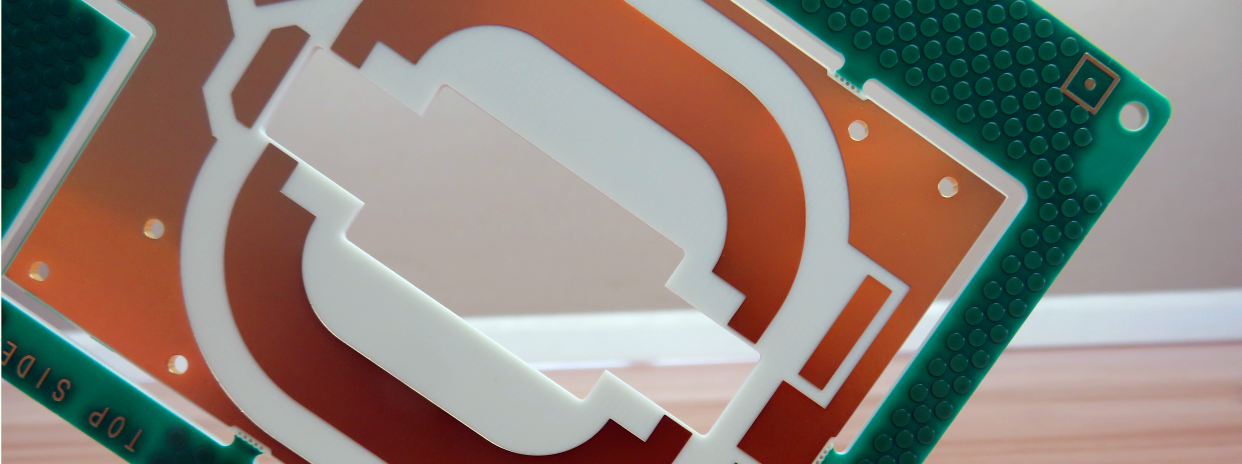
Printed Circuit Boards are custom-made products; the images and specifications provided are for reference only.
General Description
Rogers AD250C PCB is a type of double layer high frequency PCB built on Rogers AD250C antenna grade materials, featuring a dielectric constant of 2.50 and a dissipation factor of 0.0013.
This PCB has a thickness of 60mil, with 1oz copper on both sides, and is manufactured without solder mask or silkscreen. It measures 90mm by 90mm in size, with immersion gold applied to its pads for enhanced conductivity and corrosion resistance.
Fabricated strictly in accordance with IPC-Class-II standards, each board undergoes 100% electrical testing before delivery to ensure performance reliability. For shipment, 25 boards are vacuum-packed to protect against moisture and physical damage during transit.
.jpg)
PCB Specifications
| PCB SIZE | 90mm x 90mm=1 piece |
| BOARD TYPE | High Frequency PCB |
| Number of Layers | 2 layers |
| Surface Mount Components | YES |
| Through Hole Components | N/A |
| LAYER STACKUP | copper ------- 35um(1 oz)+plate top layer |
| AD250C 1.524mm | |
| copper ------- 35um(1 oz)+plate bot layer | |
| TECHNOLOGY | |
| Minimum Trace and Space: | 80 mil |
| Minimum / Maximum Holes: | 1.0 mm / 2.8 mm |
| Number of Different Holes: | 2 |
| Number of Drill Holes: | 9 |
| Number of Milled Slots: | 0 |
| Number of Internal Cutouts: | 0 |
| Impedance Control: | no |
| Number of Gold finger: | 0 |
| BOARD MATERIAL | |
| Glass Epoxy: | AD250C 1.524mm |
| Final foil external: | 2.0 oz |
| Final foil internal: | 2.0 oz |
| Final height of PCB: | 1.6 mm ±0.1 |
| PLATING AND COATING | |
| Surface Finish | Immersion Gold, 73.6% |
| Solder Mask Apply To: | Both sides |
| Solder Mask Color: | N/A |
| Solder Mask Type: | N/A |
| CONTOUR/CUTTING | Routing |
| MARKING | |
| Side of Component Legend | N/A |
| Colour of Component Legend | N/A |
| Manufacturer Name or Logo: | N/A |
| VIA | Plated through hole(PTH), minimum size 1.0mm. |
| FLAMIBILITY RATING | 94V-0 |
| DIMENSION TOLERANCE | |
| Outline dimension: | 0.0059"" |
| Board plating: | 0.0029"" |
| Drill tolerance: | 0.002"" |
| TEST | 100% Electrical Test prior shipment |
| TYPE OF ARTWORK TO BE SUPPLIED | email file, Gerber RS-274-X, PCBDOC etc |
| SERVICE AREA | Worldwide, Globally. |
Features & Benefits
- Very low loss PTFE and ceramic filled composite (0.0014 loss tangent at 10GHz)
- Dielectric constant (Dk) of 2.50 +/-0.04
- Low profile copper for lower conductive losses
- Higher antenna efficiencies
- Low PIM for antenna applications
- Powerful PCB capabilities support your research and development, sales and marketing;
- 16000㎡ workshop; 30000㎡ output capability per month; 8000 types of PCB's per month;
- ISO9001, ISO14001, IATF16949, ISO13485, UL Certified factory.
- Delivery on time higher than 98% on-time-delivery rate;
- Prototype PCB capability to Volume Production capability;
Typical Applications
1.Cellular infrastructure base station antenna
2. Automotive telematics antenna systems
3. Commercial satellite radio antenna
| Parameter | Value |
| Layer Counts | 1-32 |
| Substrate Materials | RO4350B, RO4003C, RO4730G3, RO4360G2, RO4533, RO4534, RO4535, RO4835, RO3003, RO3006, RO3010, RO3035, RO3203, RO3210; RT/Duriod 5880; RT/Duriod 5870, RT/Duriod 6002, RT/Duroid 6010, RT/duroid 6035HTC; RT/duroid 5880LZ; TMM3, TMM4, TMM6, TMM10, TMM10i, TMM13i, Kappa 438; TLF-35; RF-35TC, RF-60A, RF-60TC, RF-35A2, RF-45, RF-10, TRF-45; TLX-0, TLX-6, TLX-7, TLX-8; TLX-9, TLY-3, TLY-5, TLY-5Z; PTFE F4B (DK2.2 DK2.65 DK2.85 DK2.94, DK3.0, DK3.2, DK3.38, DK3.5, DK4.0, DK4.4, DK6.15, DK10.2); AD250C, AD255C, AD300D, AD350A, AD450, AD600, AD1000, TC350; TC600; DiClad 880, DiClad 870, DiClad 527; IsoClad 917; Nelco N4000, N9350, N9240; SCGA-500 GF220, SCGA-500 GF255, SCGA-500 GF265, SCGA-500 GF300; FR-4 ( High Tg S1000-2M, TU-872 SLK, TU-768, IT-180A etc.), FR-4 High CTI>600V; Polyimide, PET; Metal Core etc. |
| Maximum Size | Flying test: 900*600mm, Fixture test 460*380mm, No test 1100*600mm |
| Board Outline Tolerance | ±0.0059"" (0.15mm) |
| PCB Thickness | 0.0157"" - 0.3937"" (0.40mm--10.00mm) |
| Thickness Tolerance(T≥0.8mm) | ±8% |
| Thickness Tolerance(t<0.8mm) | ±10% |
| Insulation Layer Thickness | 0.00295"" - 0.1969"" (0.075mm--5.00mm) |
| Minimum Track | 0.003"" (0.075mm) |
| Minimum Space | 0.003"" (0.075mm) |
| Outer Copper Thickness | 35µm--350µm (1oz-10oz) |
| Inner Copper Thickness | 17µm--350µm (0.5oz - 10oz) |
| Drill Hole(Mechanical) | 0.0079"" - 0.25"" (0.2mm--6.35mm) |
| Finished Hole(Mechanical) | 0.0039""-0.248"" (0.10mm--6.30mm) |
| DiameterTolerance(Mechanical) | 0.00295"" (0.075mm) |
| Registration (Mechanical) | 0.00197"" (0.05mm) |
| Aspect Ratio | 12:1 |
| Solder Mask Type | LPI |
| Min Soldermask Bridge | 0.00315"" (0.08mm) |
| Min Soldermask Clearance | 0.00197"" (0.05mm) |
| Plug via Diameter | 0.0098"" - 0.0236"" (0.25mm--0.60mm) |
| Impedance Control Tolerance | ±10% |
| Surface Finish | HASL,HASL LF,ENIG,Immersion Tin,Immersion Silver, OSP, Gold Finger, Pure gold plated etc. |